
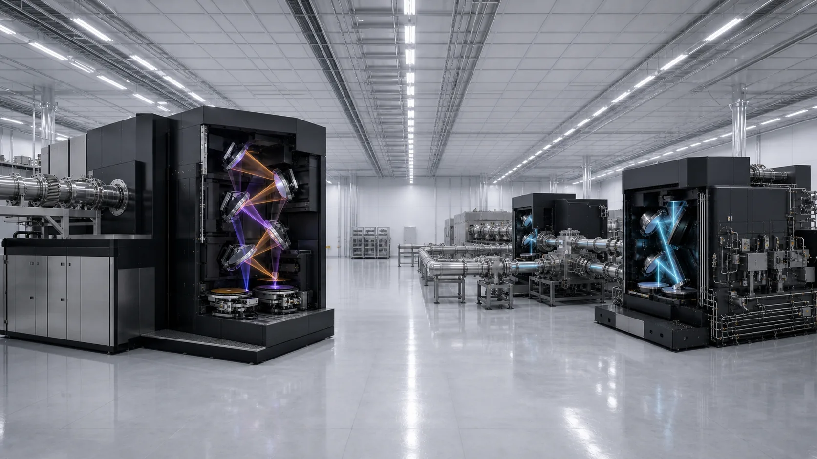
Final consolidated pre-concept report
Prepared by Claude Code and Codex as equal Nexus Co-Lab collaborators under the directive of the human operator. Research cut-off: 12 August 2026.
Status: This is a falsifiable engineering study, not an ASML product, an ASML-endorsed roadmap, or a build-ready design. Calculated values are model results or engineering allocations unless a cited source reports a measurement.
Executive answer
We came up with two machine designs after re-reading the first lithography report, reading the internal-photon-randomness concept, researching the missing technical questions, and forcing both designs through the same optical, stochastic, thermal, throughput, and economic tests.
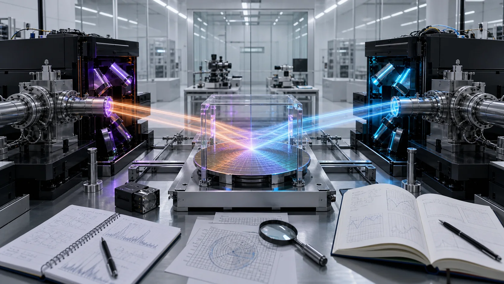
First, the terminology must be exact:
- 6.65 nm is the proposed exposure wavelength. It is selected by the useful material window just above the boron K edge and is the standard beyond-EUV region considered here.
- 6 nm is the target printed half-pitch. It is not the exposure wavelength.
- A marketing node name is neither of those quantities.
The two machines are:
- Design A, Q6 Sentinel: a 6.65 nm, NA 0.45 scanner that attacks stochastic error through higher image contrast. It uses a new La/B-based optical column, a 6.65 nm phase-reticle programme, a boron-based pellicle branch, and a dense inorganic resist and dry-process branch. It reaches 6 nm half-pitch with modeled
k1 = 0.406, 32.84 nm Rayleigh depth of focus, and a photon-only edge sigma of 0.2954 nm at 40 mJ/cm2 if aerial NILS reaches 3.5. - Design B, E13 Photon Foundry: a 13.5 nm scanner family that attacks stochastic error by making photons abundant through a shared ERL-FEL light utility. B1 keeps NA 0.55 as a lower-risk 8 nm yield bridge. B2 uses a new NA 0.75 hyper-NA projection system to reach 6 nm half-pitch with modeled
k1 = 0.333. B2 matches Design A's photon-only sigma at 76.76 mJ/cm2 if aerial NILS remains near 2.0, but it pays with 24.0 nm depth of focus, at least 6x slit demagnification in the first-order bandwidth model, 255 fields per wafer, polarized illumination, a new hyper-NA optic, and a chemical-noise floor that dose cannot remove.
The central conclusion is not that one design has already won. Two cheap measurements decide the choice:
- Gate A, image slope: Can the 6.65 nm phase-reticle system deliver aerial NILS at or above 2.53 against the modeled B2 equal-dose competitor? The older 2.17 threshold remains the separate crossover against today's 8 nm High-NA photon-only sigma.
- Gate B, dose saturation: On an existing High-NA tool, does total roughness and electrical defectivity keep improving with dose, or does a non-photon floor appear? If a floor is at or above the target sigma, no finite dose makes Design B reach the target.
If Gate A passes and Gate B finds a material floor, Design A is the stronger architecture. If Gate A fails and Gate B finds no limiting floor, Design B is the stronger architecture. If both pass, cost per good wafer decides. If both fail, neither single-exposure 6 nm route is ready.
Part I. What changed after the two reports were combined?
1. What did the first report establish?
The first report established a 6.65 nm platform called Q6 Sentinel. Its main insight was that stochastic edge error depends differently on image contrast and photon count:
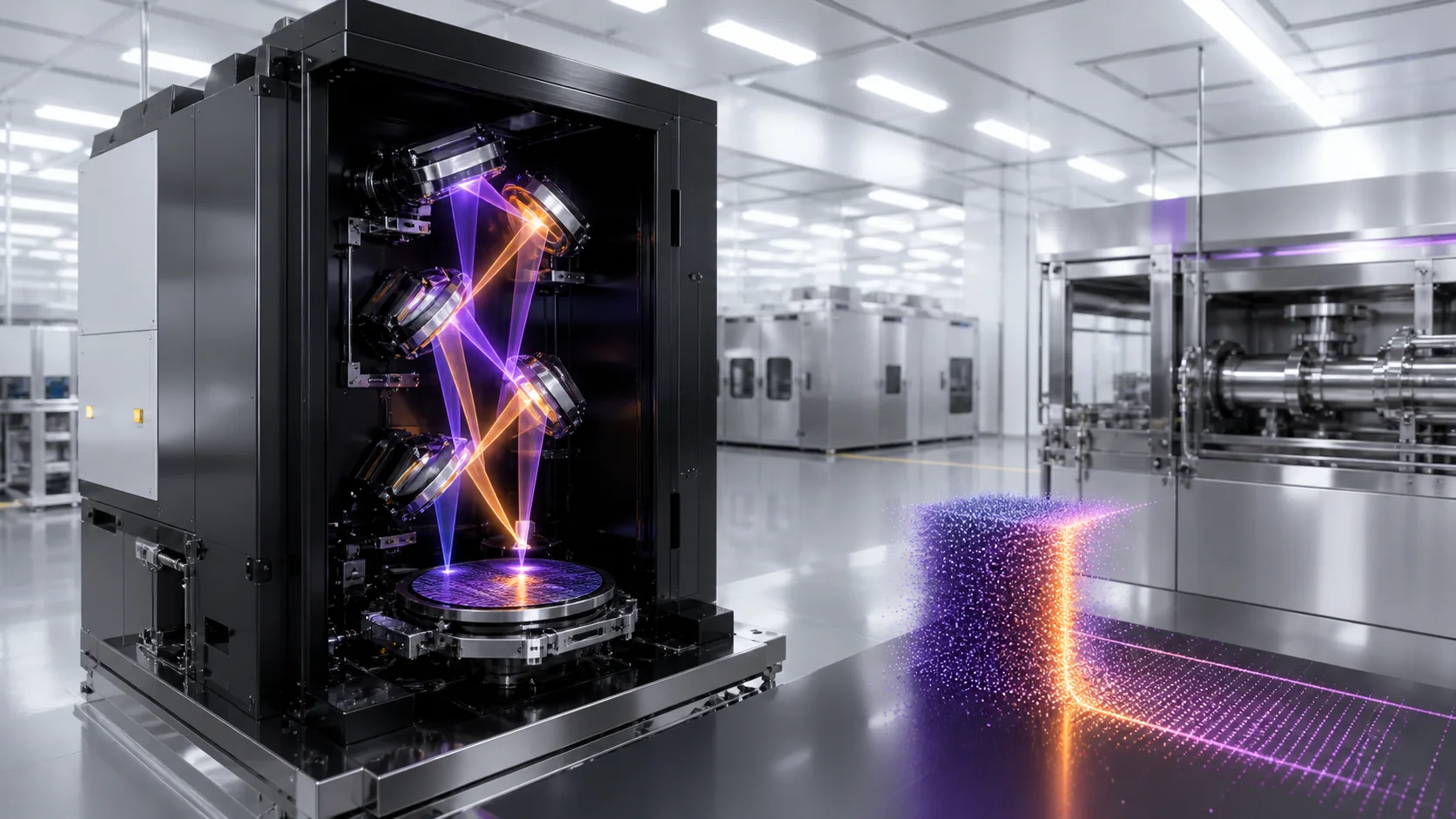
sigma_EPE = CD / (NILS_eff * sqrt(Phi_abs * A_corr))In this first-order shot-noise model:
CDis the critical dimension or half-pitch under comparison.NILS_effis aerial-image slope after the resist-blur transfer penalty.Phi_absis absorbed photon density.A_corris the assumed correlation area.
Image slope enters linearly. Photon count enters through a square root. Q6 therefore spends a wavelength change on higher k1 and higher contrast rather than trying to buy every improvement through dose.
The first report also established that literal 6.00 nm exposure is the wrong target for this material system. At 6.00 nm the photon energy is about 206.6 eV, above the boron K edge near 188.1 eV. The useful La/B-based normal-incidence multilayer window is around 6.6 to 6.7 nm, not 6.00 nm. IRDS likewise treats 6 nm < wavelength < 7 nm as the beyond-EUV region and states that it requires a new source, reflective coatings, and resists. IEEE IRDS 2024 Lithography and Patterning
2. What did the internal-dice concept add?
The second report made a different argument. Photon arrival is fundamentally random, but the damage caused by that randomness depends on how many photons are affordable. A shared accelerator light plant could replace a separate tin-plasma source in every scanner, remove the collector and debris system, and make high dose economically plausible.
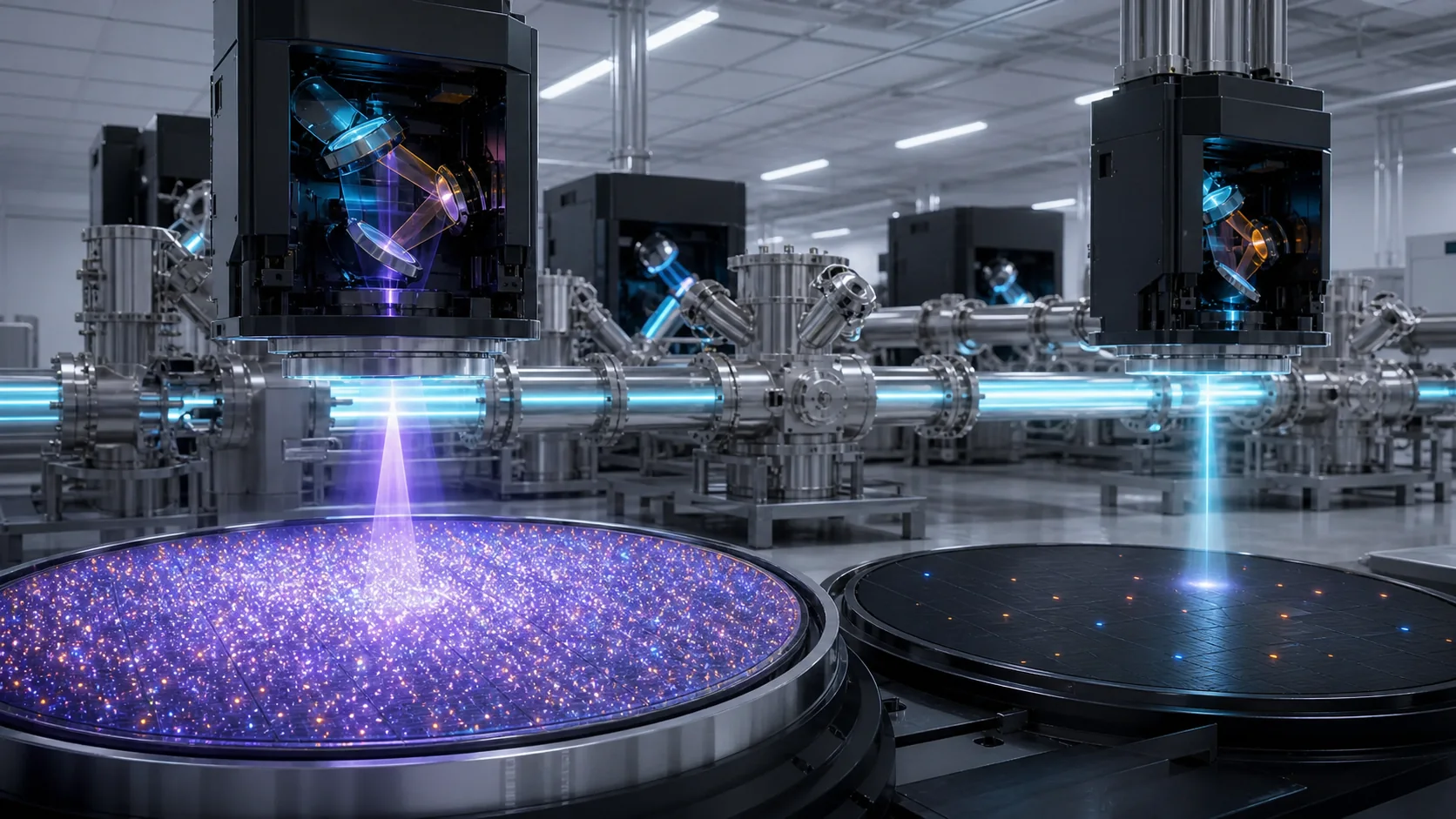
That argument attacks the square-root term of the same equation. The first report had treated dose as expensive under a plasma-source economy, then selected an accelerator for Q6 without fully re-evaluating what accelerator abundance could do at 13.5 nm.
The combined study closes that gap. It also discovers that Design B has two materially different generations:
- B1 buys better stochastic margin at the current 8 nm High-NA resolution.
- B2 combines abundance with hyper-NA, so it can compete with Q6 at the same 6 nm half-pitch.
3. What was corrected during peer review?
The two-agent review changed the conclusion in both directions:
- Codex initially stated that Design A alone could single-expose 6 nm. Claude's B2 model disproved that statement. Codex independently reproduced B2 and withdrew the claim.
- Claude initially credited B2 with 9.1 active scanners per 10 kW source plant. Codex applied B2's own 255-field overhead and reduced the figure to 5.4 at 150 WPH. Claude independently reproduced the correction and updated the model.
- The original Q6
NILS >= 2.17gate was not arithmetically wrong, but it compared Q6 at 6 nm with today's High-NA platform at 8 nm. The new 6 nm-to-6 nm equal-dose comparison producesNILS >= 2.53. The final report names both benchmarks. - Design B was initially described as using qualified parts. That is valid only for many B1 material families. B2 retains the established 13.5 nm material ecosystem but needs an unbuilt hyper-NA projection system, a new mask format, polarization engineering, and full qualification.
- The internal-dice essay suggested photon power could be raised by 10 to 50 times. The combined model shows something sharper: Design B reaches modeled parity below 1 kW at scanner entry, so an accelerator is not required for parity. The accelerator buys dose above parity and multi-scanner fanout. Large dose remains limited by heat, field time, source fanout, and the non-photon floor.
Part II. The common physics
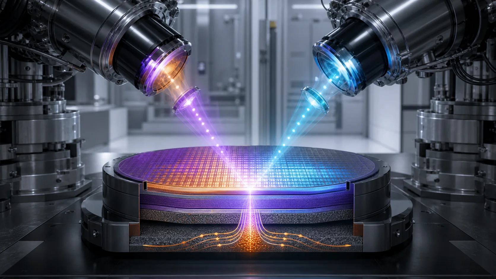
4. Why does shorter wavelength lose photons at equal energy dose?
Photon energy is:
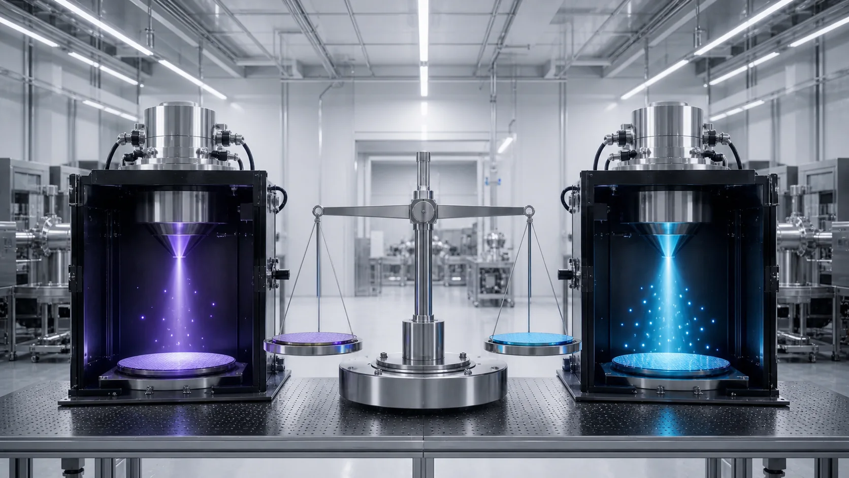
E_photon = hc / wavelengthAt 13.5 nm, photon energy is about 91.84 eV. At 6.65 nm, it is about 186.44 eV. At equal energy dose, 6.65 nm therefore supplies roughly half as many incident photons.
| Wavelength and dose | Incident photons per nm2 |
|---|---|
| 13.5 nm at 40 mJ/cm2 | 27.18 |
| 6.65 nm at 40 mJ/cm2 | 13.39 |
| 6.65 nm at about 81.2 mJ/cm2 | about 27.18 |
IRDS expresses the same physical penalty by stating that maintaining equal photon shot noise at 6 to 7 nm requires roughly twice the energy at the wafer, if optical efficiency and other conditions are held. IEEE IRDS 2024 Lithography and Patterning
Q6 accepts that penalty because it expects a larger gain from image slope. E13 accepts current image slope and buys photon count.
5. Why is photon-only sigma not total defectivity?
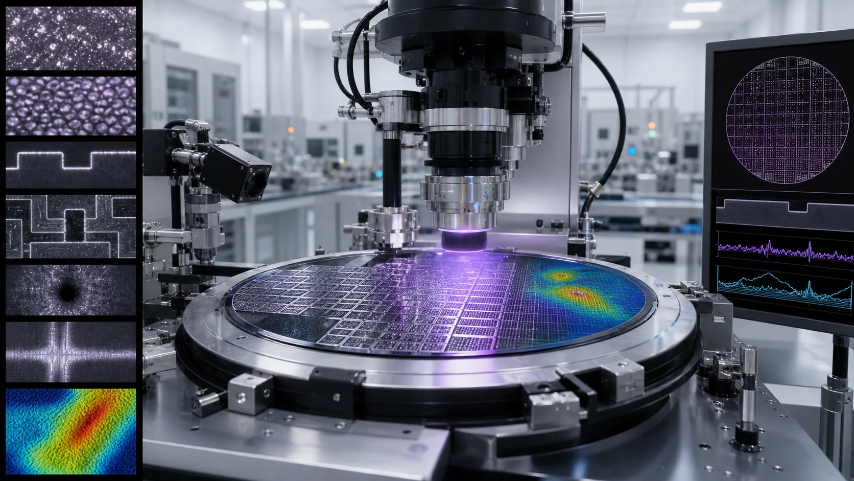
The analytic model contains the photon-count term and a Gaussian blur transfer factor. It does not contain the full stochastic process:
- photon arrival;
- absorption position;
- primary and secondary-electron generation;
- electron transport;
- molecular, cluster, sensitizer, or quencher distributions;
- reaction statistics;
- diffusion or cross-linking;
- development and pattern collapse;
- mask roughness and flare;
- underlayer and etch transfer;
- local thermal and focus state;
- rare non-Gaussian bridge, break, missing-hole, and merged-hole tails.
The two architectures move those terms differently:
| Randomness or error term | Design A, Q6 Sentinel | Design B, E13 Photon Foundry |
|---|---|---|
| Photon arrival | attacks it through higher NILS at higher k1 | attacks it through dose until a residual floor dominates |
| Secondary-electron cascade | partly reduced by dense, short-range film design | substantially inherited from the 13.5 nm process stack |
| Electron transport blur | partly reduced by the new inorganic chemistry branch | substantially inherited |
| Molecular, sensitizer, and quencher statistics | deletes conventional PAG and quencher statistics if the non-CAR branch succeeds | keeps them in the baseline resist family |
| Diffusion or cross-linking | replaces acid diffusion with a different, still unproven short-range reaction path | keeps the established chemical-amplification trade space |
| Development and collapse | attacks it with dry, self-limiting processing | retains it unless a different process module is qualified |
| Source pulse jitter | reduced by accelerator pulse averaging | reduced identically by the same accelerator class |
| Coherent speckle | new accelerator risk | the same new accelerator risk |
| Mask roughness and defects | uses higher demagnification but must build 6.65 nm actinic infrastructure | retains 13.5 nm actinic knowledge but pays a new B2 mask format |
| Mask 3D effects | phase-reticle branch aims to suppress absorber shadowing | thinner optical absorber in wavelength units, but worse hyper-NA angles |
| Mirror roughness and flare | creates a roughly 0.04 nm RMS polishing requirement | keeps the much less punitive 13.5 nm scatter scaling |
| Overlay, stage, and thermal state | budgeted around a conservative 120 mJ/cm2 qualification point | worsens as dose rises and the B2 exposure window shrinks |
A 2024 imec review states that stochastic failures are partly caused by photon shot noise and also by resist chemistry, underlayer interaction, image contrast, mask imperfections, track processing, and etch. It also reports typical EUV process doses around 35 to 50 mJ/cm2. Ronse, Continued dimensional scaling through projection lithography
For that reason, every sigma in the head-to-head calculation is labeled a photon-only floor, not a prediction of product defect density.
6. Why can dose stop paying?
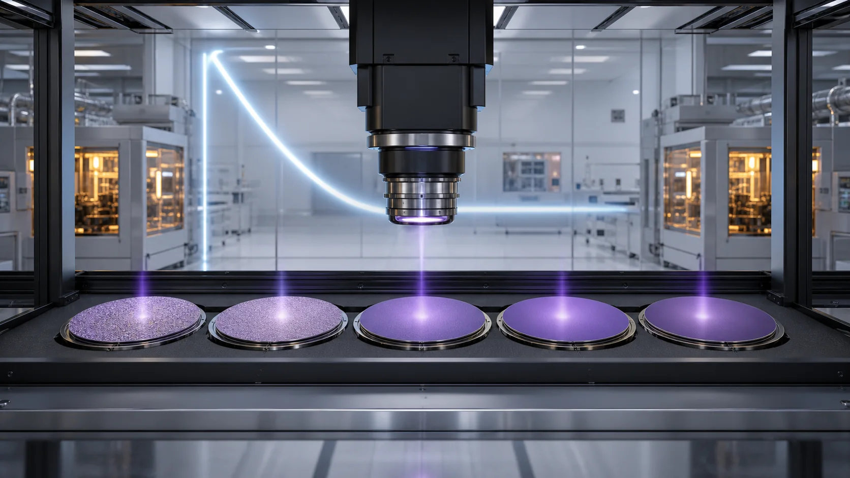
A bounded sensitivity model separates the dose-reducible photon term from an unknown residual term:
sigma_total(D)^2 = sigma_photon,40^2 * (40 / D) + sigma_floor^2Solving for dose at a target sigma gives:
D_required = 40 * sigma_photon,40^2
             / (sigma_target^2 - sigma_floor^2)
This is not proof that the residual is constant. It is a deliberately simple boundary test. Its most important result is exact: if sigma_floor equals or exceeds sigma_target, the denominator is zero or negative and no finite dose reaches the target.
For B2, using the shared photon model and a target of 0.2954 nm:
| Assumed residual sigma floor | Required B2 dose | Energy over 650 cm2 | Upper-bound uncooled wafer rise |
|---|---|---|---|
| 0.00 nm | 76.76 mJ/cm2 | 49.89 J | 0.559 K |
| 0.10 nm | 86.69 mJ/cm2 | 56.35 J | 0.631 K |
| 0.20 nm | 141.72 mJ/cm2 | 92.12 J | 1.032 K |
| 0.25 nm | 270.53 mJ/cm2 | 175.84 J | 1.969 K |
| 0.28 nm | 756.17 mJ/cm2 | 491.51 J | 5.504 K |
| 0.2954 nm or more | no finite dose | not applicable | not applicable |
The numbers above are a sensitivity sweep, not measured process behavior. They show why the dose-ladder experiment is load-bearing.
The abundance route creates the regime in which its own limiting assumption first becomes testable. A residual floor can be hidden when the photon term dominates at ordinary process doses. It separates cleanly only when the ladder is extended toward roughly 100 to 400 mJ/cm2, the range where the model's alternatives diverge. Under a photon-scarce source economy there has been little reason to spend that dose. Gate B is therefore not a confirmation exercise. It is the first direct look at the operating point on which both machine choices depend.
Part III. Design A, Q6 Sentinel
7. What is Q6 Sentinel?
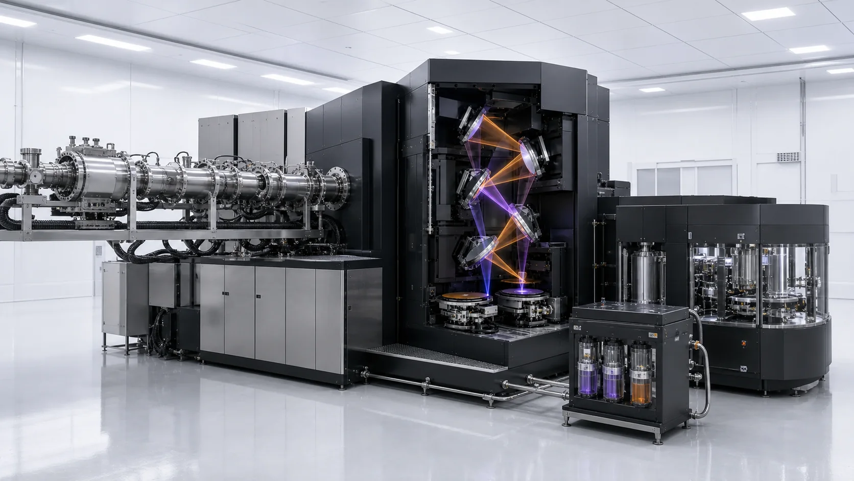
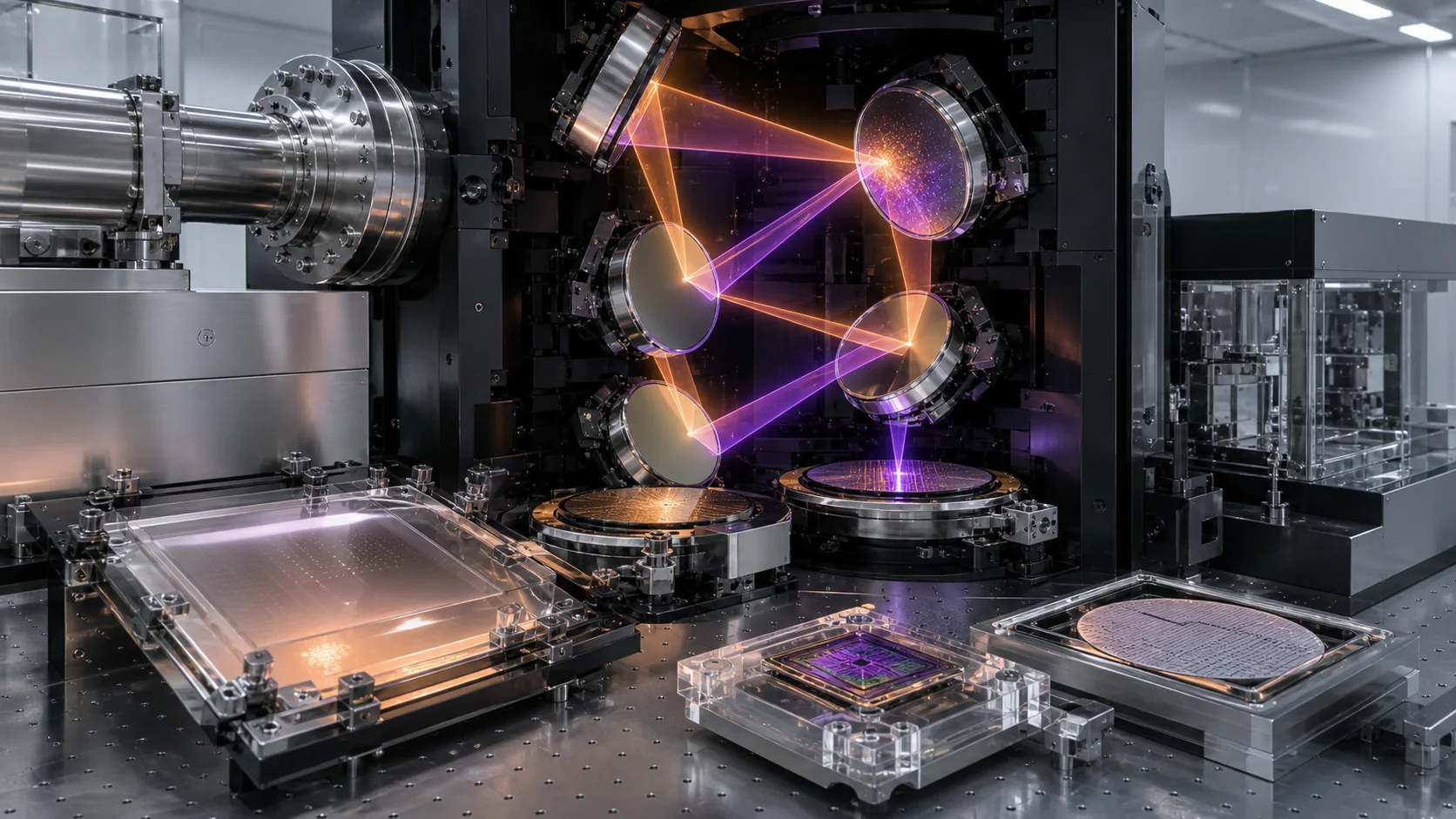
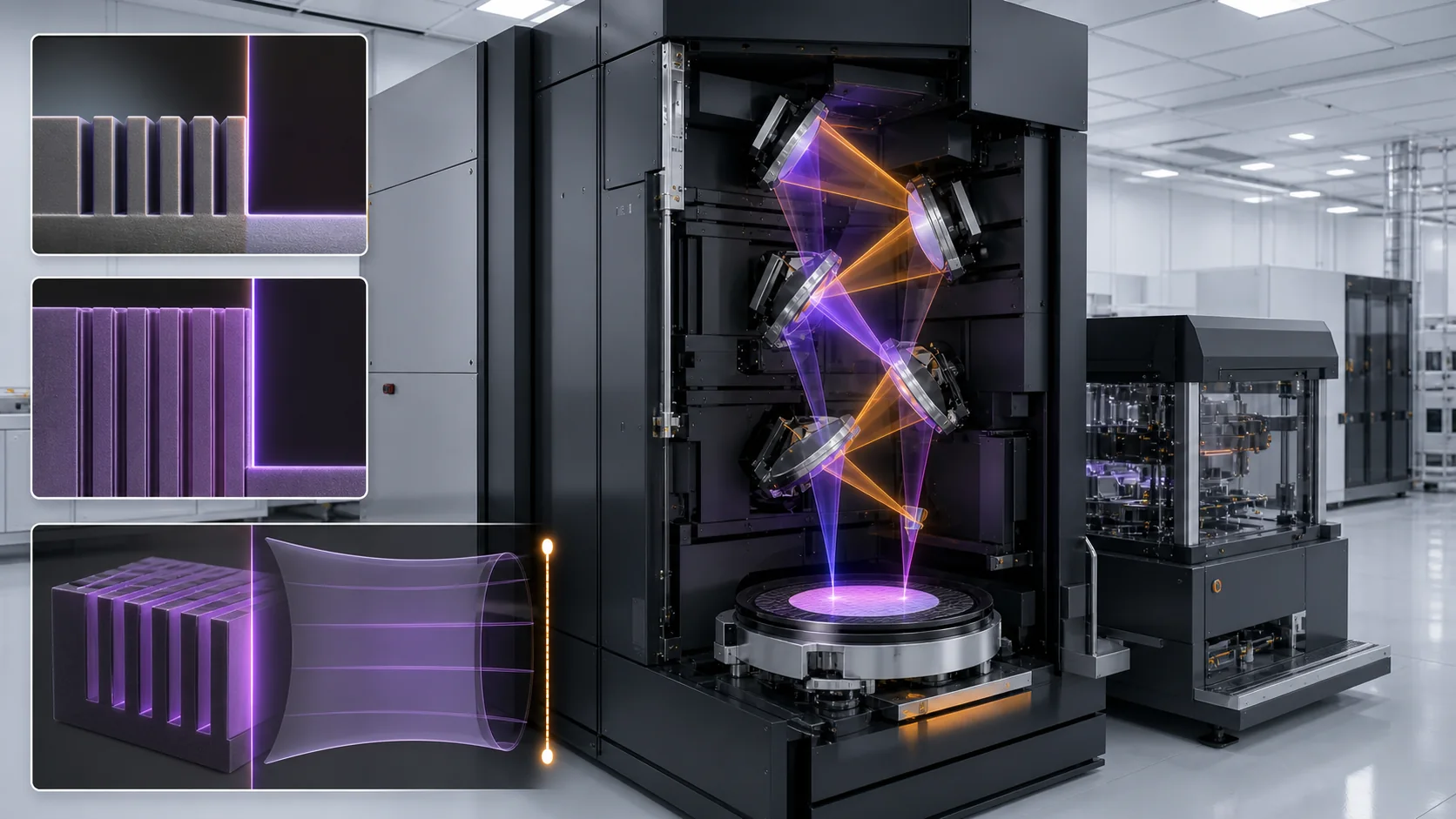
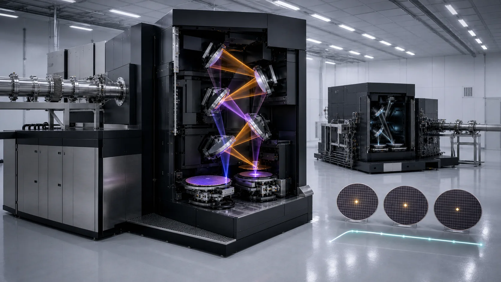
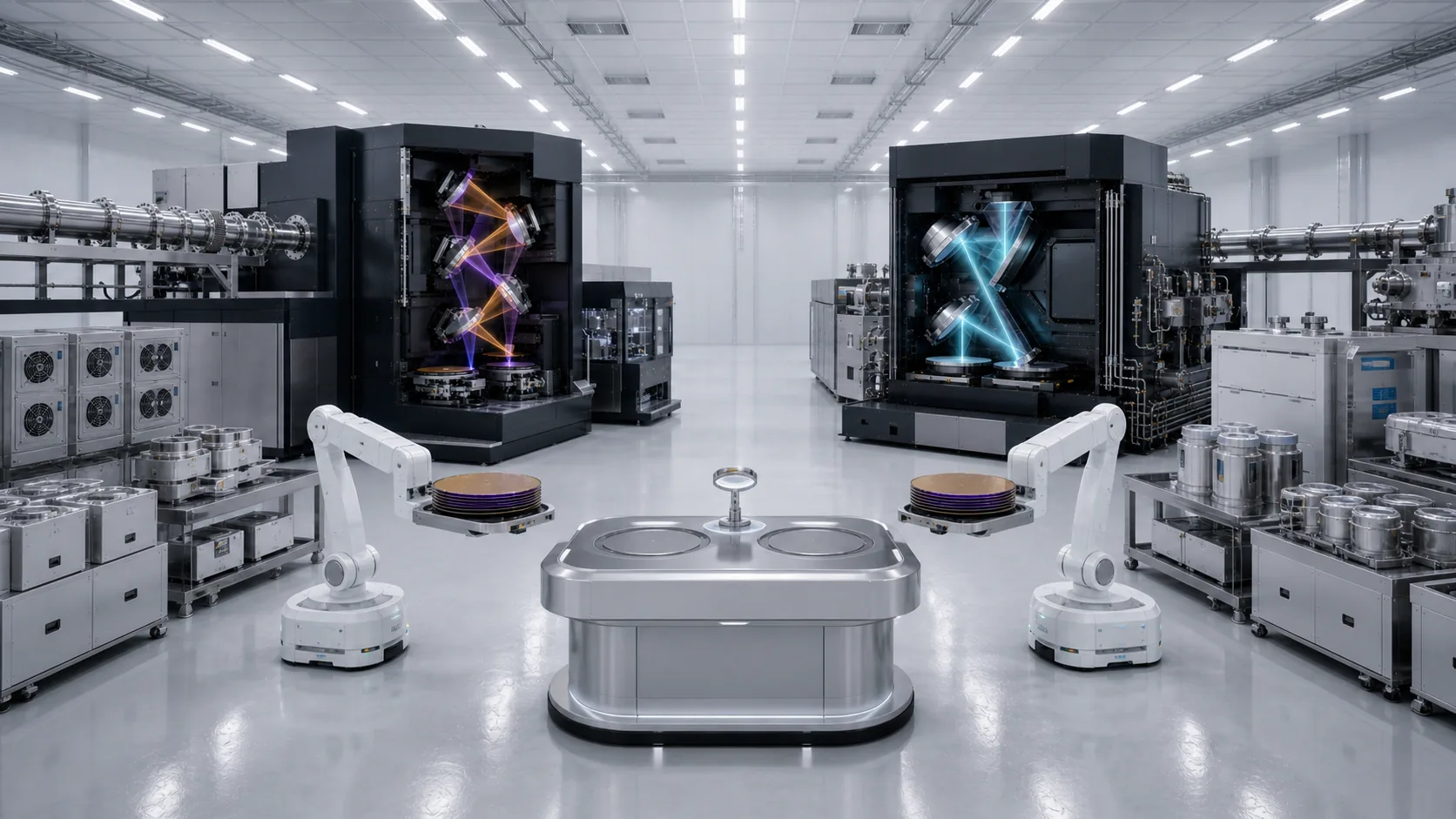
Q6 Sentinel is a resonance-aligned 6.65 nm reflective scanner designed to reach 6 nm half-pitch while improving the photon-only edge-error floor through image contrast.
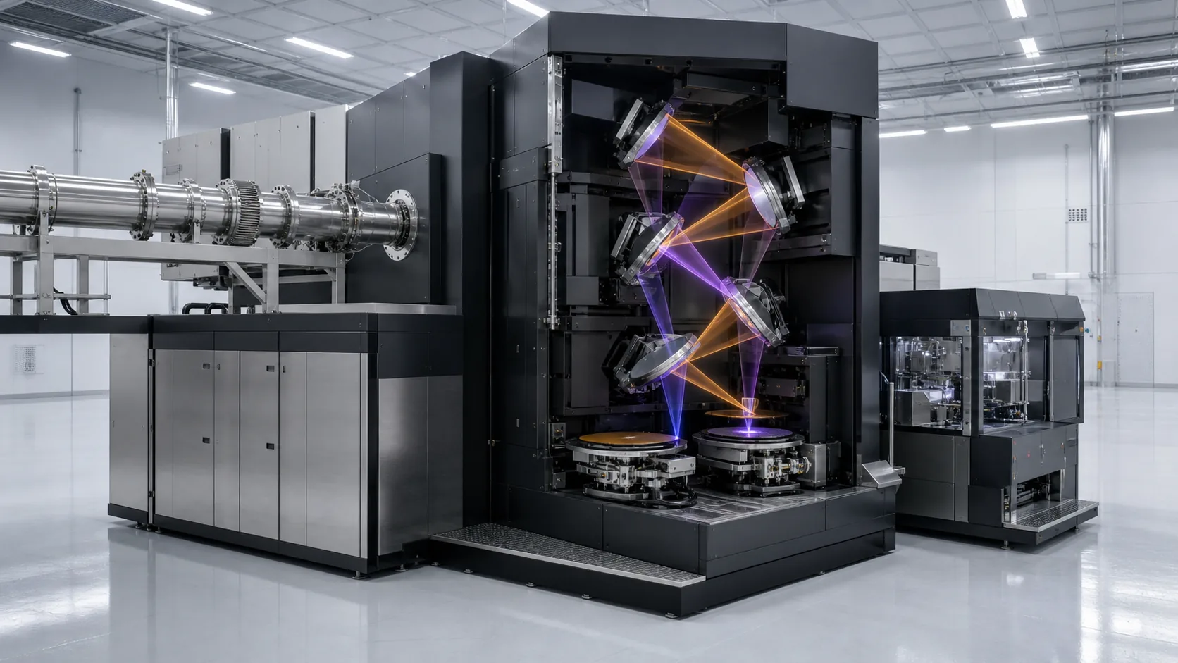
Baseline architecture
[6.65 nm ERL-FEL utility with N+1 redundancy]
                       |
[grazing transport, fast isolation, spectrum and energy pickoff]
                       |
[coherence conditioning, programmable pupil, polarization control]
                       |
[8x scan / 4x slit reticle, phase-mask lead branch, B-based pellicle]
                       |
[six-mirror La/B-based projection optics, NA 0.45]
                       |
[dual wafer stage, mapped focus, grid, temperature, and dose controls]
                       |
[dense Zn-rich inorganic imaging branch, dry development branch]
Planning specification
| Parameter | Q6 Sentinel planning value |
|---|---|
| Exposure wavelength | 6.65 nm |
| Wafer-side NA | 0.45 |
| Single-exposure half-pitch | 6.0 nm target |
k1 at target | 0.4060 |
Rayleigh DOF, k2 = 1 | 32.84 nm |
| Reticle format | 8x scan / 4x slit, 26 x 16.5 mm wafer field |
| Projection mirrors | 6 |
| Full-angle coating budget | 55% to 60% per broadened surface |
| Pure-optics transmission model | 0.1266% from scanner entry to wafer |
| Aerial NILS assumption | 3.5, unproven |
| Photon-only sigma at 40 mJ/cm2 | 0.2954 nm |
| Qualification dose | 120 mJ/cm2 conservative test point |
| Economic dose objective | 20 to 40 mJ/cm2 after measured gates |
| Overlay allocation | 0.553 nm at 3 sigma against a 0.70 nm concept ceiling |
8. Why is the wavelength 6.65 nm?
The candidate optical stack needs a low-loss spacer and a strong scatterer. Around 6.65 nm, boron is still below its K absorption edge while lanthanum provides strong optical contrast. Published La/B-based multilayer work measured 64.1% reflectance at 6.65 nm and 1.5 degrees off normal on a periodic coupon. That is important evidence, but it is not full-pupil, aperiodic, thermally loaded scanner performance. Kuznetsov et al., Optics Letters 40, 3778
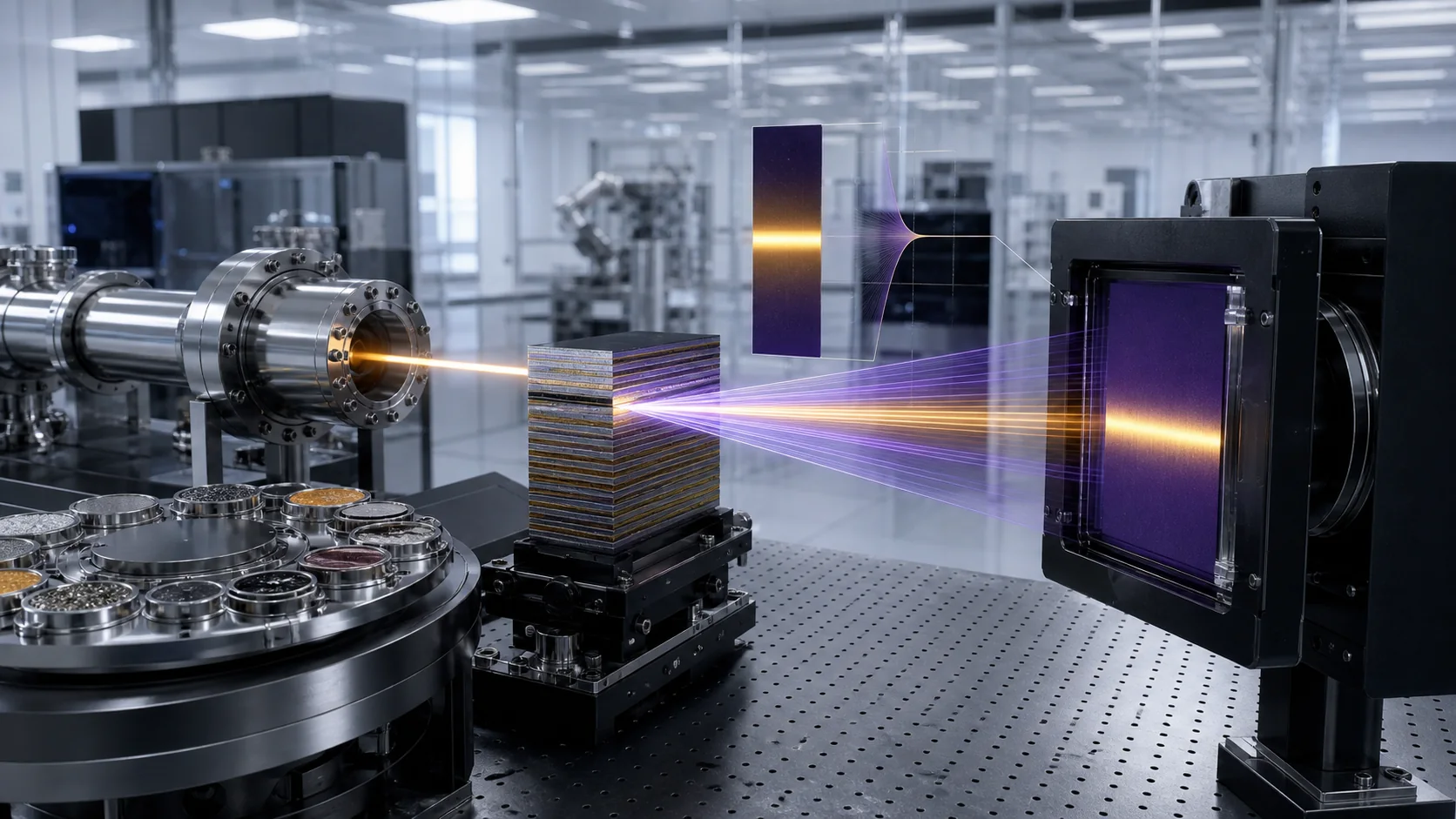
The same wavelength creates a materials cascade:
- B and B4C are candidates for spacers and pellicles.
- La/B-based multilayers become the projection-coating family.
- Zn remains an attractive resist absorber while tin absorption falls sharply relative to 13.5 nm.
- Lanthanide absorbers and emitters become relevant near their resonances.
These statements begin with tabulated optical constants. Solid-state films near absorption edges can differ substantially, so measured film spectra are mandatory. CXRO atomic scattering factors
9. What are Q6's main advantages?
- Higher contrast at the same printed feature. Q6 uses the wavelength to raise
k1rather than spending the entire gain on NA. - More depth of focus than B2. The first-order comparison is 32.84 nm for Q6 against 24.0 nm for 13.5 nm at NA 0.75.
- Lower dose for equal photon-only sigma. Q6 uses 40 mJ/cm2 in the comparison while B2 requires 76.76 mJ/cm2.
- A path to delete process noise terms. The proposed continuous inorganic film, lack of freely diffusing photoacid, and dry self-limiting development are intended to remove molecular-count, acid-diffusion, and wet-development terms. This advantage is architectural but unproven.
- Moderate wafer-side NA. NA 0.45 avoids part of the mirror-size, asphere, polarization, and DOF pressure of hyper-NA.
10. What are Q6's hardest risks?
Coating bandwidth and reflectivity
The 64.1% measurement is a near-normal periodic coupon. Q6 needs broadened reflectance over the full angle, polarization, aperture, temperature, contamination state, and lifetime. A 55% to 60% planning value is an allocation, not a measured scanner result.
Mirror roughness and flare
Scatter scales approximately as (4 pi sigma / wavelength)^2. Halving wavelength roughly quadruples scatter for the same high-spatial-frequency roughness. The first report estimated that Q6 needs roughly 0.039 nm rms HSFR to reproduce the scatter level of 0.08 nm rms at 13.5 nm. That is an order-of-magnitude requirement pending a full roughness power-spectral-density propagation, but it is still the most severe optical fabrication risk.
Phase reticle
The lead branch uses an etched-multilayer or low-topography phase solution to improve NILS and reduce mask 3D effects. No 6.65 nm reticle has demonstrated the required image slope, defect inspection, repair, cleaning, and lifetime.
Resist
The most relevant published beyond-EUV resist evidence is an amorphous zinc-imidazolate film deposited by atomic or molecular layer deposition. The work demonstrates beyond-EUV interaction and reports residue-free development at 181 mJ/cm2, but not the dense-film, 20 to 40 mJ/cm2, low-blur process Q6 requires. Waltz et al., Chemistry of Materials 37, 8548
Source maturity
An ERL-FEL can match a narrow multilayer band and provide polarization, rapid pulse structure, and high average power. It is not fab-qualified. Q6 also needs around 1.1 GeV rather than the 800 MeV used in the published 13.5 nm design basis.
Part IV. Design B, E13 Photon Foundry
11. What is E13 Photon Foundry?
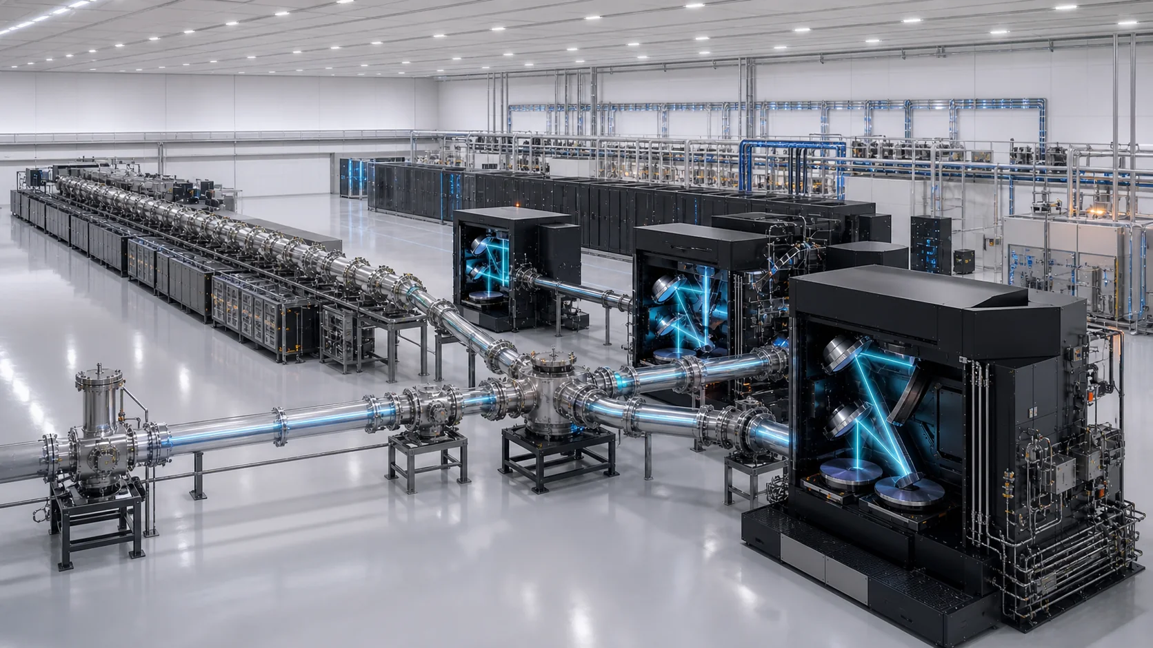
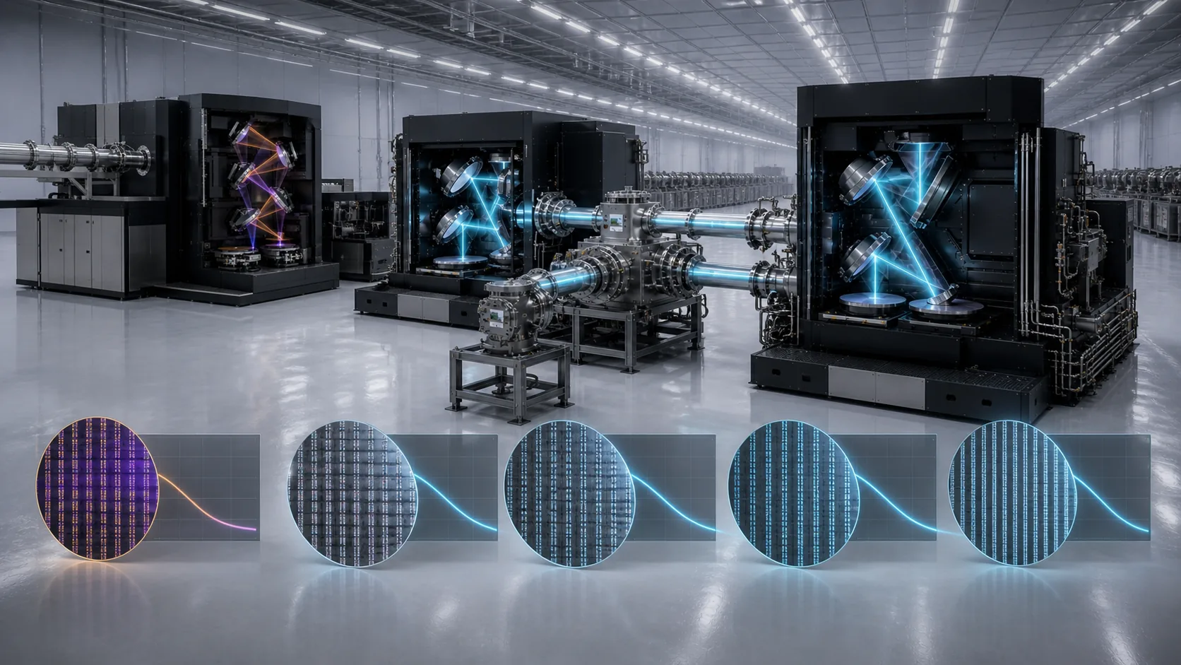
E13 Photon Foundry keeps the 13.5 nm material ecosystem and replaces separate tin-plasma sources with a shared, redundant ERL-FEL light utility. Its purpose is to turn photon supply from a scarce per-tool component into a fab service.
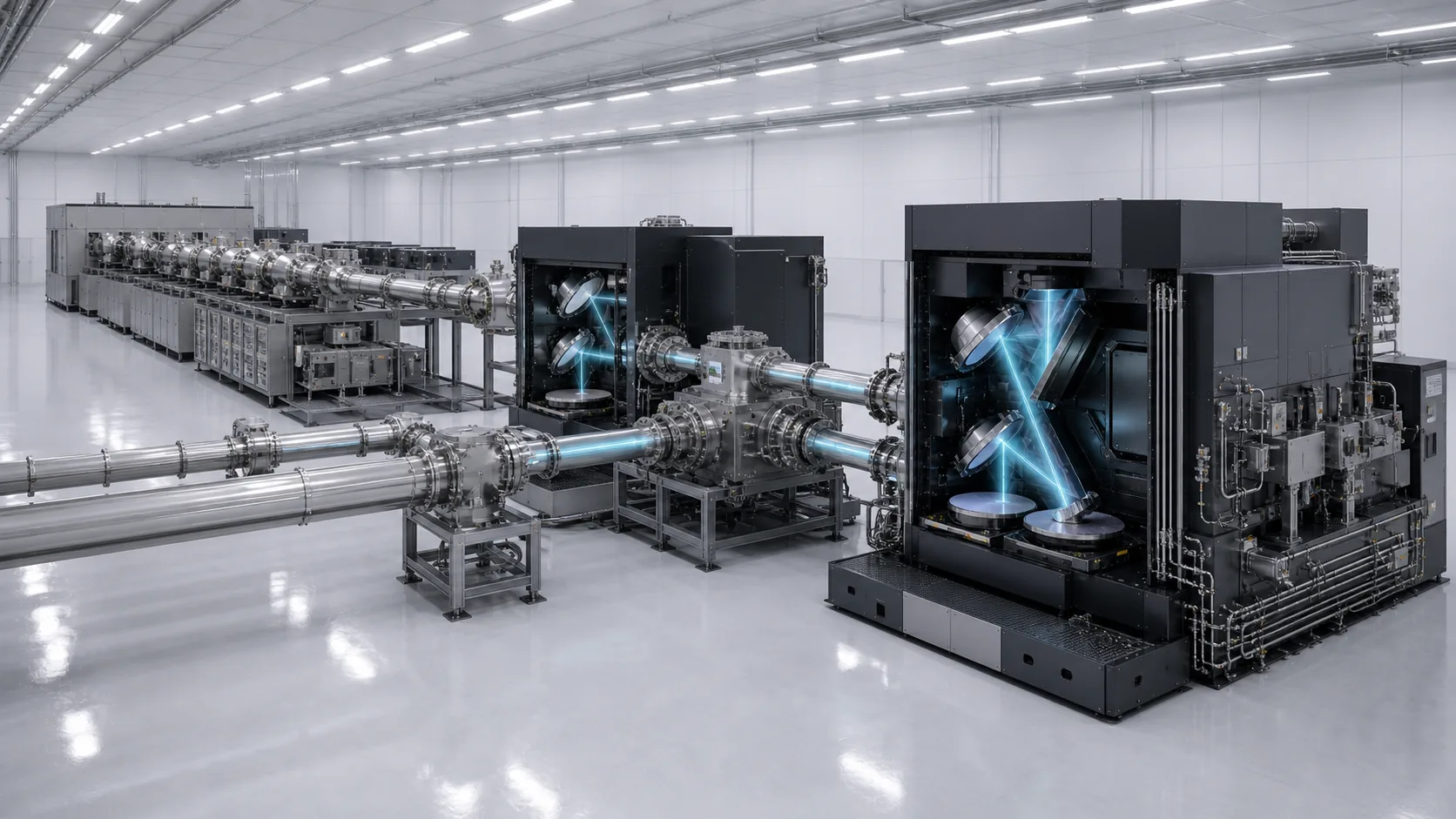
[13.5 nm ERL-FEL plant, redundant source paths]
                       |
[vacuum switchyard, beam transport, fast isolation]
                       |
[per-scanner coherence conditioning, pupil and polarization control]
                       |
       +---------------+----------------+
       |                                |
[B1, NA 0.55]                    [B2, NA 0.75]
[8 nm yield bridge]              [6 nm target]
       |                                |
[170-field format]               [at least 6x slit, 255 fields]
       +---------------+----------------+
                       |
[dual stages, zoned chuck, dose floor, electrical-yield feedback]
The ERL-FEL concept is grounded in serious accelerator engineering, but the published 10 kW-class 13.5 nm system remains a design. Konomi et al. describe an 800 MeV, 9.75 mA, 60 pC, 162.5 MHz ERL-FEL cavity design and its higher-order-mode damping requirements. The paper does not demonstrate 10 kW output, semiconductor uptime, scanner fanout, or product imaging. Konomi et al., Physical Review Accelerators and Beams 26, 121601
12. What is B1, the High-NA bridge?
B1 retains a 0.55 NA High-NA class projection platform and targets 8 nm half-pitch. It is the lower-integration-risk route because it keeps the current wavelength, coating family, and basic imaging format.
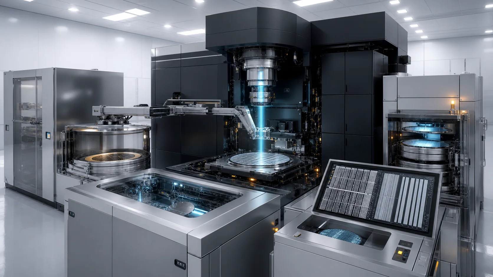
The shared model gives:
13.5 nm, NA 0.55, 8 nm half-pitch
sigma at 40 mJ/cm2 = 0.4767 nm
photon-only dose for sigma 0.2954 nm = 104.18 mJ/cm2
B1 produces the same absolute photon-only edge sigma as Q6 while printing a 33% larger feature. It is therefore a yield and robustness machine, not the final 6 nm machine.
ASML describes the EXE:5200B as a 0.55 NA platform with 8 nm resolution and 40% more imaging contrast than NXE systems. The product page states that throughput is rated at 50 mJ/cm2. ASML's 2025 annual report publishes 175 WPH for the EXE:5200B. The dose basis and platform facts were directly checked; the 175 numeral is treated here as an industry-published anchor, not a result independently measured or extracted by both agents. ASML EXE:5200B, ASML 2025 annual report
13. What is B2, the hyper-NA target?
B2 is the serious 6 nm competitor to Q6. It keeps 13.5 nm but raises NA to 0.75:
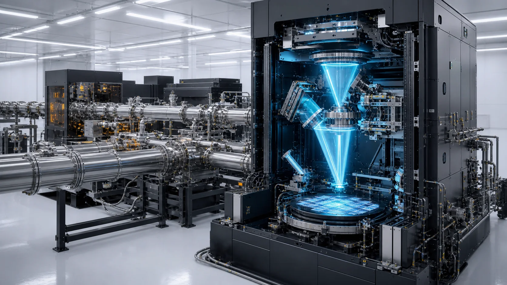
13.5 nm, NA 0.75, 6 nm half-pitch
k1 = 0.3333
Rayleigh DOF = 24.0 nm
assumed aerial NILS = 2.0
photon-only sigma at 40 mJ/cm2 = 0.4092 nm
dose for photon-only sigma 0.2954 nm = 76.76 mJ/cm2
This result is valid inside the shared analytic model and survived an independent reimplementation. It is not proof that a real hyper-NA mask and projection system delivers NILS 2.0.
Why does B2 need a new mask format?
The mask-side ray cone expands with wafer-side NA. Using the first report's Bragg-spread convention and an approximate 4.4% Mo/Si bandwidth:
| Configuration | Mask NA | Estimated Bragg spread | Result |
|---|---|---|---|
| High-NA 0.55, 4x slit | 0.1375 | 4.26% | near the modeled limit |
| Hyper-NA 0.75, 4x slit | 0.1875 | 7.67% | exceeds the modeled limit |
| Hyper-NA 0.75, 6x slit | 0.1250 | 3.56% | first workable branch |
| Hyper-NA 0.75, 8x slit | 0.09375 | 2.08% | more margin, smaller field |
This is a first-order estimate, not a transfer-matrix or full-pupil design. It says B2 cannot simply inherit the current 4x slit format. At 6x, the modeled field area falls from 4.29 to 2.86 cm2 and the field count rises from 170 to 255.
Why is B2 not made from only qualified parts?
B2 reuses the established 13.5 nm material family, but it still requires:
- an unbuilt 0.75 NA projection system with larger mirrors and stronger aspheres;
- a new 6x-or-higher slit reduction and mask qualification;
- polarized illumination and vector-imaging validation;
- tighter focus, wafer-flatness, and resist-thickness control for 24 nm DOF;
- FEL coupling and coherence conditioning;
- thermal requalification at the selected dose;
- a measured proof that total stochastic error does not saturate before the target.
IRDS describes hyper-NA as reusing the basic 13.5 nm infrastructure while still requiring larger optical elements and improvements in polishing, coating, metrology, focus control, and polarized light. IEEE IRDS 2024 Lithography and Patterning
14. What are Design B's main advantages?
- A much more transmissive optical chain in the model. The 13.5 nm pure-optics model is 0.9448%, against 0.1266% for Q6, a factor of about 7.5.
- Existing wavelength material knowledge. Mo/Si coatings, 13.5 nm mask materials, pellicles, resist families, actinic inspection, and contamination practice carry much more evidence than their 6.65 nm counterparts.
- No 0.039 nm roughness requirement caused by wavelength halving. At the same roughness, 13.5 nm has about one quarter of the first-order scatter term of 6.65 nm.
- Accelerator benefits transfer. High repetition rate, narrow bandwidth, programmable polarization, source-pulse averaging, no tin collector, and source sharing benefit B as well as A.
- Parity does not require the accelerator. At 150 WPH, the field-aware model needs about 0.79 kW at scanner entry for B1 and 0.93 kW for B2 at their parity doses. Even if the calibrated optical chain is two or three times too optimistic, those figures become about 1.58 or 2.36 kW for B1 and 1.85 or 2.78 kW for B2. A 10 kW-class light plant earns its place by buying dose margin above parity and by feeding several scanners, not by making parity possible.
- A staged product path. B1 can test source, coherence, thermal, and economic assumptions before B2's hyper-NA optic exists.
15. What are Design B's hardest risks?
- The non-photon floor. Dose cannot remove a floor at or above the target sigma.
- Hyper-NA feasibility. B2 needs a projection system that does not exist and a real pupil and mask design that confirms NILS and angular acceptance.
- Field-count penalty. The smaller field shortens the exposure window at fixed WPH and raises instantaneous power.
- Thermal strain. High dose converts a random photon problem into systematic wafer, reticle, and optics distortion.
- Shared-source availability. A facility source is a common-mode failure unless the architecture has N+1 source capacity, isolated beam paths, and unambiguous wafer disposition.
- FEL coherence. Speckle and standing-wave structure must be decorrelated or homogenized without destroying transmission or contrast.
- Capital concentration. Source economics work only if enough scanners share the plant without losing availability.
Part V. Head-to-head engineering comparison
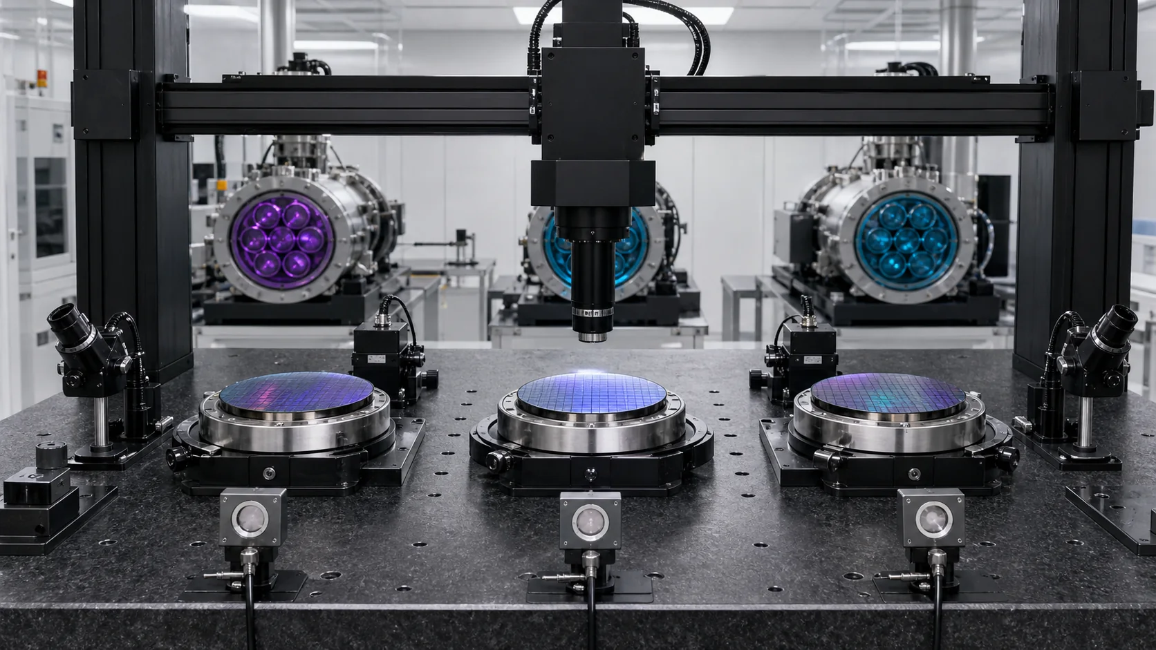
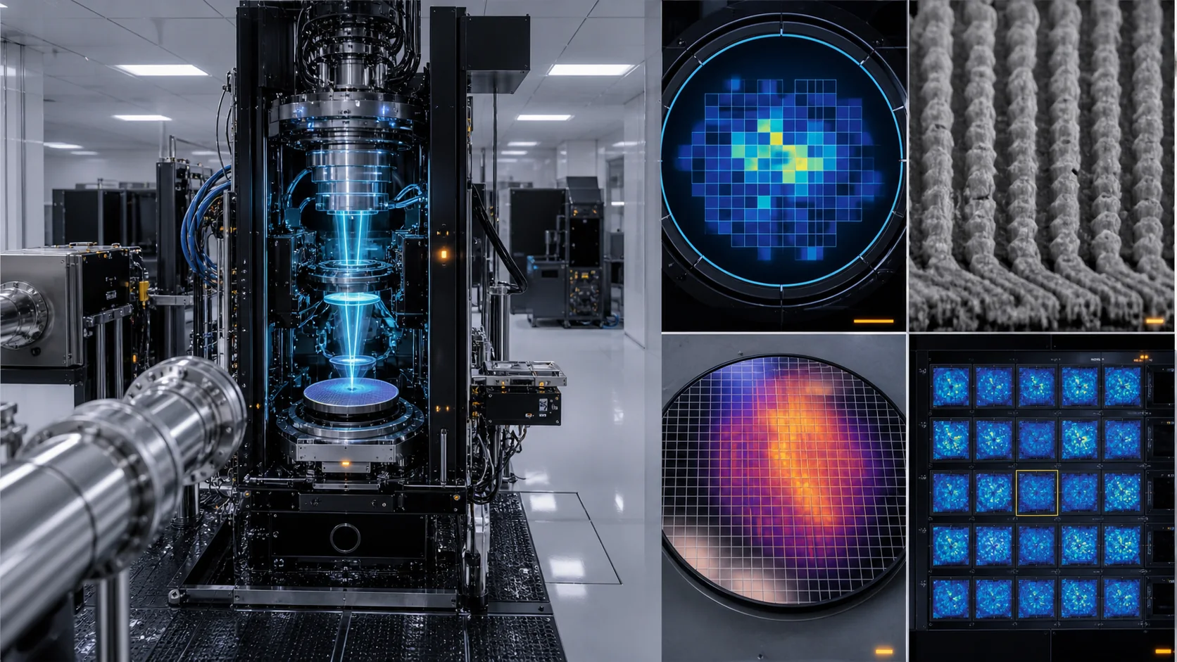
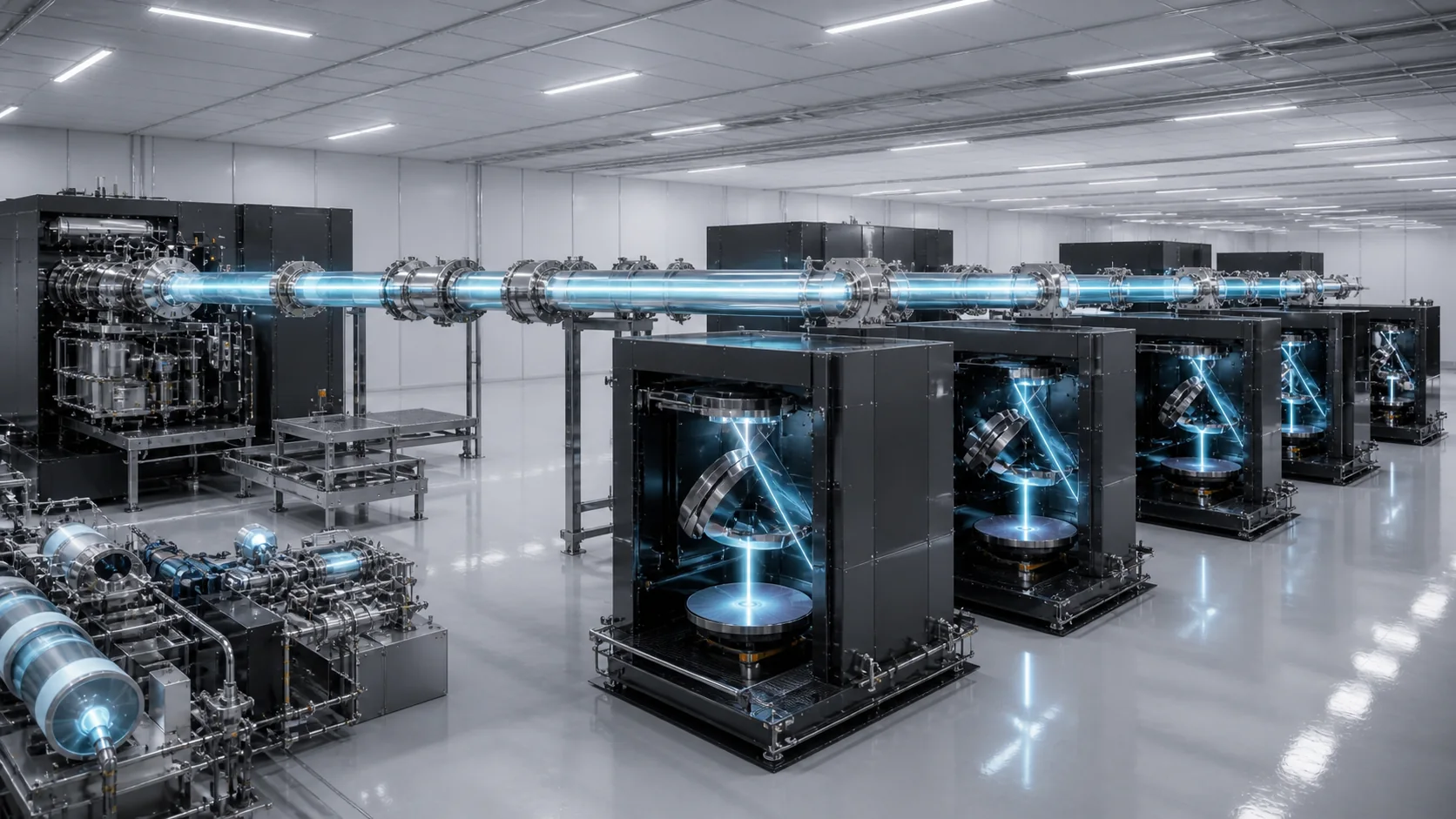
16. What does one controlled model say?
The following table uses identical photon statistics, resist-blur convention, 650 cm2 patterned area, 0.85 productivity derating, 40 ms field turnaround, 4.5 s swap and calibration, and each architecture's optical and field assumptions.
| Quantity | Design A, Q6 | Design B1, High-NA bridge | Design B2, hyper-NA target |
|---|---|---|---|
| Wavelength | 6.65 nm | 13.5 nm | 13.5 nm |
| NA | 0.45 | 0.55 | 0.75 |
| Half-pitch | 6.0 nm | 8.0 nm | 6.0 nm |
k1 | 0.406 | 0.326 | 0.333 |
| Rayleigh DOF | 32.84 nm | 44.63 nm | 24.00 nm |
| Aerial NILS assumption | 3.5 | 2.0 | 2.0 |
| Dose for 0.2954 nm photon-only sigma | 40.00 mJ/cm2 | 104.18 mJ/cm2 | 76.76 mJ/cm2 |
| Energy over 650 cm2 | 26.00 J | 67.72 J | 49.89 J |
| Upper-bound uncooled wafer rise | 0.291 K | 0.758 K | 0.559 K |
| Field count | 170 | 170 | 255 |
| Exposure window at 150 WPH | 9.10 s | 9.10 s | 5.70 s |
| Usable wafer power at 150 WPH | 2.86 W | 7.44 W | 8.75 W |
| Scanner-entry power at 150 WPH | 2.26 kW | 0.79 kW | 0.93 kW |
| Facility allocation at 50% transport | 4.52 kW | 1.58 kW | 1.85 kW |
| Active scanners per 10 kW facility | 2.2 | 6.3 | 5.4 |
These fanout numbers are active-exposure power limits, not connected-tool counts, uptime predictions, or economic forecasts. They exclude N+1 spare capacity, guard bands, rejected pulses, pointing and spectrum losses beyond the planning model, maintenance, and switchyard scheduling.
17. Why did the B2 fanout correction matter?
The first B2 model used Design A's fixed 0.40 exposure duty fraction. That produced 0.55 kW scanner entry and 9.1 active scanners per plant. B2's own 6x slit result then raised field count to 255, which increased turnaround from 6.8 to 10.2 seconds and shortened the exposure window.
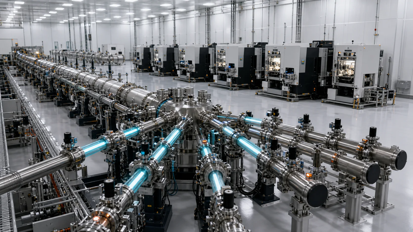
At 150 WPH the consistent B2 values are 0.93 kW at scanner entry and 5.4 active scanners per 10 kW facility. At 175 WPH, only 2.786 seconds remain for exposure, raising the values to 1.90 kW at scanner entry and 2.64 active scanners per facility.
This correction did not eliminate B2. It removed an internally inconsistent advantage and made the comparison credible.
18. What does the thermal analysis prove?
The simple temperature rises prove only that dose energy is large enough to require explicit control. They do not predict the field-scale transient.
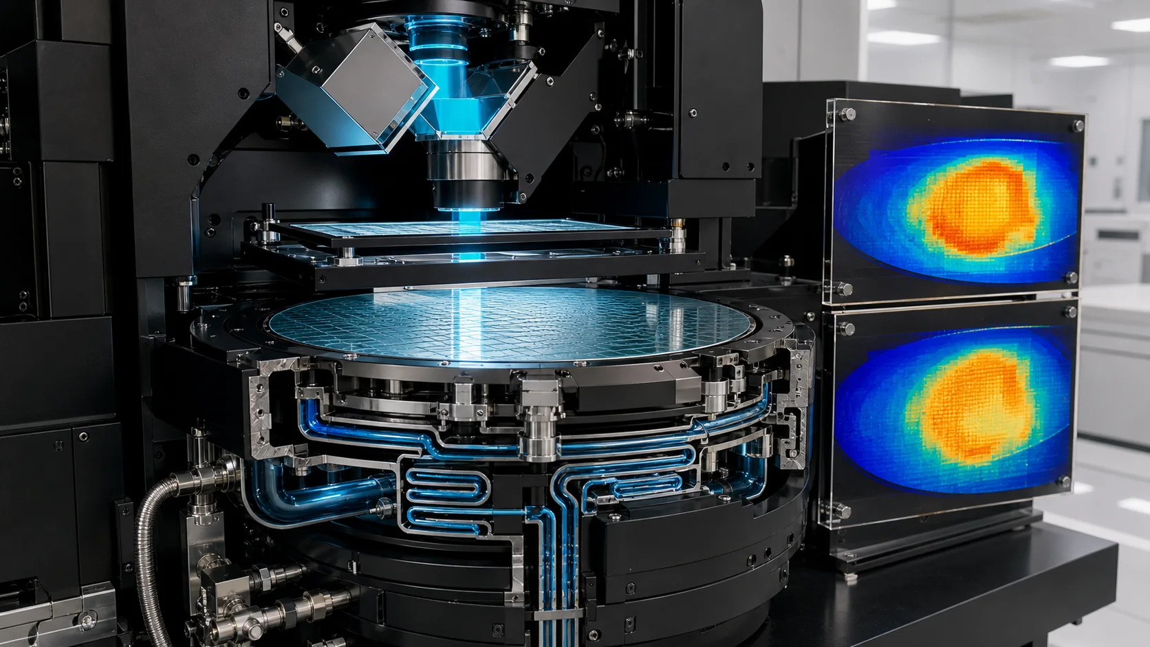
Finite-element literature establishes that EUV absorption can create wafer temperature and displacement changes that affect placement and blur, with strong sensitivity to chuck contact conductance. A 2023 model reported scan-dependent local deformation up to about 1.5 nm in its modeled die, which is larger than the sub-nanometer overlay budgets considered here. Chang, Engelstad, and Lovell, Ko et al.
Reticle heating is already a material overlay contributor at current EUV power. A 2024 study specifically examines reticle thermal properties at powers above 500 W. Higher dose and new source illumination therefore require new absorption maps, chuck-temperature control, feed-forward correction, and validation. Huddleston et al.
Both designs need:
- zoned, high-conductance electrostatic wafer chucks;
- calibrated backside contact maps and contamination inspection;
- heat-distributing scan order;
- reticle layout-derived absorption maps;
- pulse-to-field absorbed-power history;
- temperature and strain sentinels;
- model-predictive focus and wafer-grid correction;
- a hard hold if the thermal state leaves the qualified range.
The functional gate is not average wafer temperature. It is measured overlay, CD, focus, and electrical yield through first-wafer-after-idle, long-lot, source-interruption, and restart conditions.
19. How should cost be compared?
No credible sale price exists for either pre-concept machine. The right metric is:
cost per good wafer =
  (annualized scanner capital
   + source-facility share
   + N+1 redundancy
   + transport and switchyard
   + service, electricity, cooling
   + masks, pellicles, resist, process modules, inspection)
  /
  (WPH * 8760 * availability * utilization * electrical yield)
The adoption rules are:
- Q6 must replace enough multipatterned work or recover enough yield to pay for the new wavelength ecosystem.
- B1 must improve 8 nm electrical yield enough to pay for the source utility, cooling, and common-mode redundancy.
- B2 must beat Q6 and multipatterning after the hyper-NA optic, smaller field, polarization, thermal controls, and measured defect floor are charged.
Resolution alone is not an economic case. Photon-only sigma alone is not a yield case.
Part VI. The two decisive gates
20. What is Gate B, and why should it run first?
Gate B asks whether dose keeps paying in a real High-NA resist process.
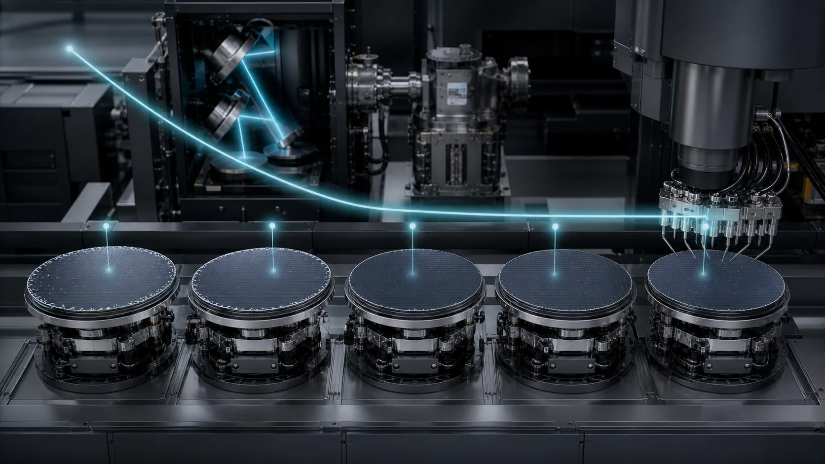
Run a 30 to 400 mJ/cm2 dose ladder on an installed High-NA tool with at least one production-relevant metal-oxide resist and one alternative chemistry. For every dose, measure:
- aerial and resist image metrics;
- LER, LWR, LCDU, and placement error;
- nanobridge, nanobreak, missing-hole, and merged-hole rates;
- pattern transfer through hard mask and etch;
- metallized serpentine and fork-fork electrical yield;
- wafer-grid, focus, CD, and thermal history.
Fit photon-only, dose-dependent material, and residual terms without forcing the residual to zero. Report confidence intervals and correlation, not only a best-fit sigma.
Imec's 2025 High-NA validation demonstrates the right end-to-end pattern: metal-oxide resist, pattern transfer, metallization, e-beam inspection, and electrical serpentine and fork-fork structures. That result exceeded 90% yield on 20 nm-pitch test structures, which is encouraging but not a 6 nm half-pitch or extreme-tail demonstration. imec High-NA electrical-yield result
Gate B should run first because it needs no new wavelength, coating, accelerator, or scanner. It can retire or strengthen the abundance architecture using existing hardware.
21. What is Gate A, and why are there two NILS numbers?
Gate A measures the real aerial image slope of a 6.65 nm mask and optical branch through focus, dose, pitch, orientation, polarization, field, and relevant pattern classes.
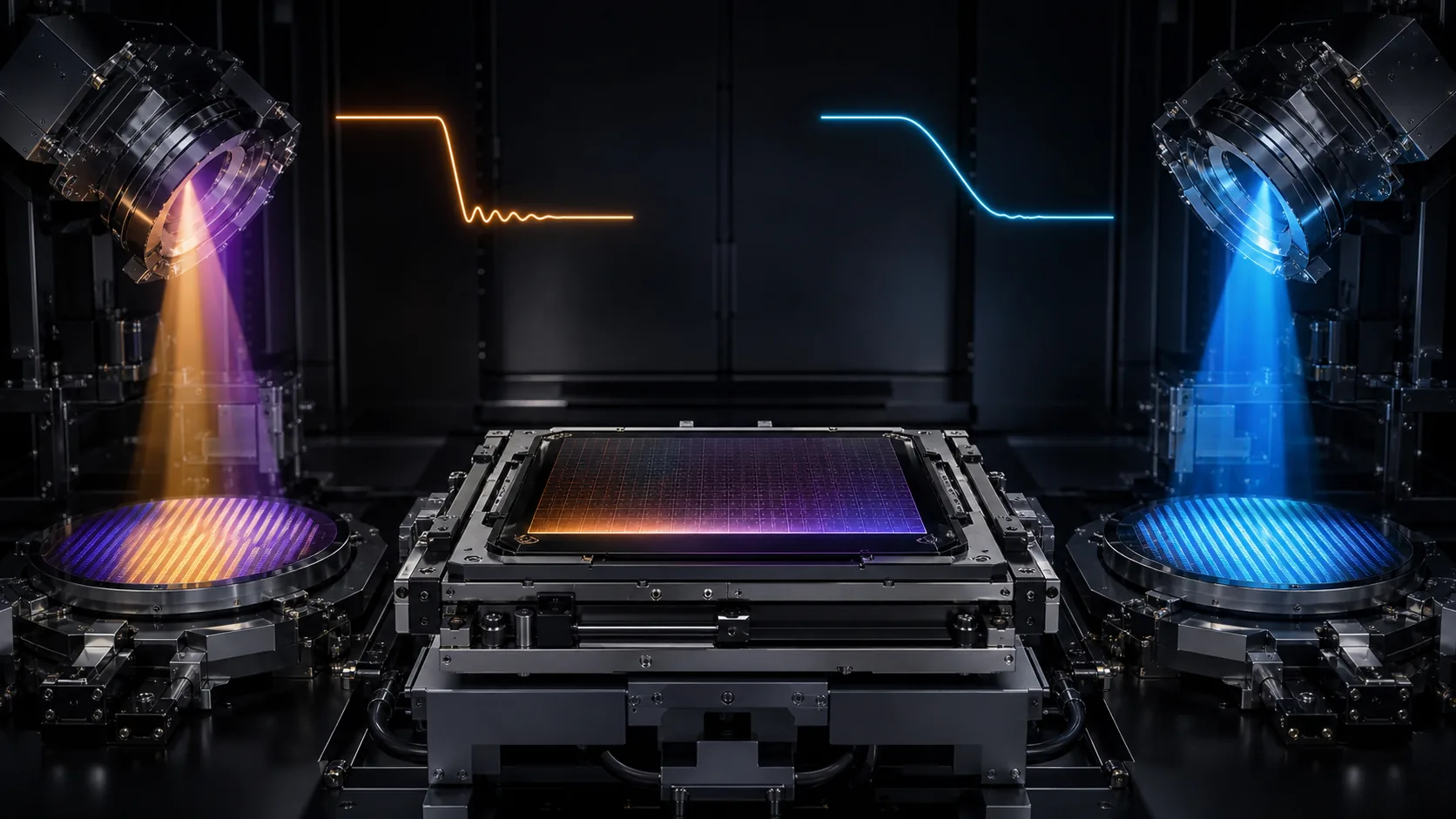
Two different comparisons produce two valid thresholds:
| Q6 aerial NILS threshold | Comparison answered |
|---|---|
| 2.17 | Q6 at 6 nm beats today's 8 nm High-NA absolute photon-only sigma at the same dose |
| 2.53 | Q6 at 6 nm beats modeled B2 at 6 nm photon-only sigma at the same dose |
The 6 nm architecture decision uses 2.53. The 2.17 value remains useful as a historical and transition benchmark. Neither threshold proves cost competitiveness, and the B2 threshold moves if the real hyper-NA NILS differs from the assumed 2.0.
Gate A should proceed in stages:
- rigorous electromagnetic mask and pupil simulation;
- measured multilayer reflectivity and phase over angle and polarization;
- 6.65 nm microfield exposure with line, contact, line-end, fork, jog, and curvilinear patterns;
- measured NILS, focus, flare, mask-defect sensitivity, and resist response;
- electrical structures after pattern transfer.
The microfield phase does not need a production accelerator. A beamline or low-power 6.65 nm plasma source can answer the decisive image-slope and resist questions first.
22. What decision does the two-gate matrix produce?
| Gate A, Q6 aerial NILS at or above 2.53 | Gate B, no limiting floor before economic dose | Engineering consequence |
|---|---|---|
| pass | pass | Both 6 nm routes remain. Choose by measured cost per good wafer and process window. |
| pass | fail | Design A is favoured because contrast and process-noise deletion are needed beyond the dose ceiling. |
| fail | pass | Design B2 is favoured if the hyper-NA optic, mask format, DOF, and thermal gates pass. |
| fail | fail | Neither single-exposure 6 nm route is ready. Retain B1 for 8 nm yield work and reopen multipatterning, resist, or another architecture. |
Part VII. Development roadmap
23. What should be built first?
Phase 0, discriminate the architectures
- Run Gate B on installed High-NA hardware.
- Measure absorption and electron response of candidate dense films at 6.6 to 6.7 nm.
- Run Gate A electromagnetic simulation.
- Model a real B2 hyper-NA pupil, mask, polarization state, field, and projection system.
Phase 1, component evidence
For Q6:
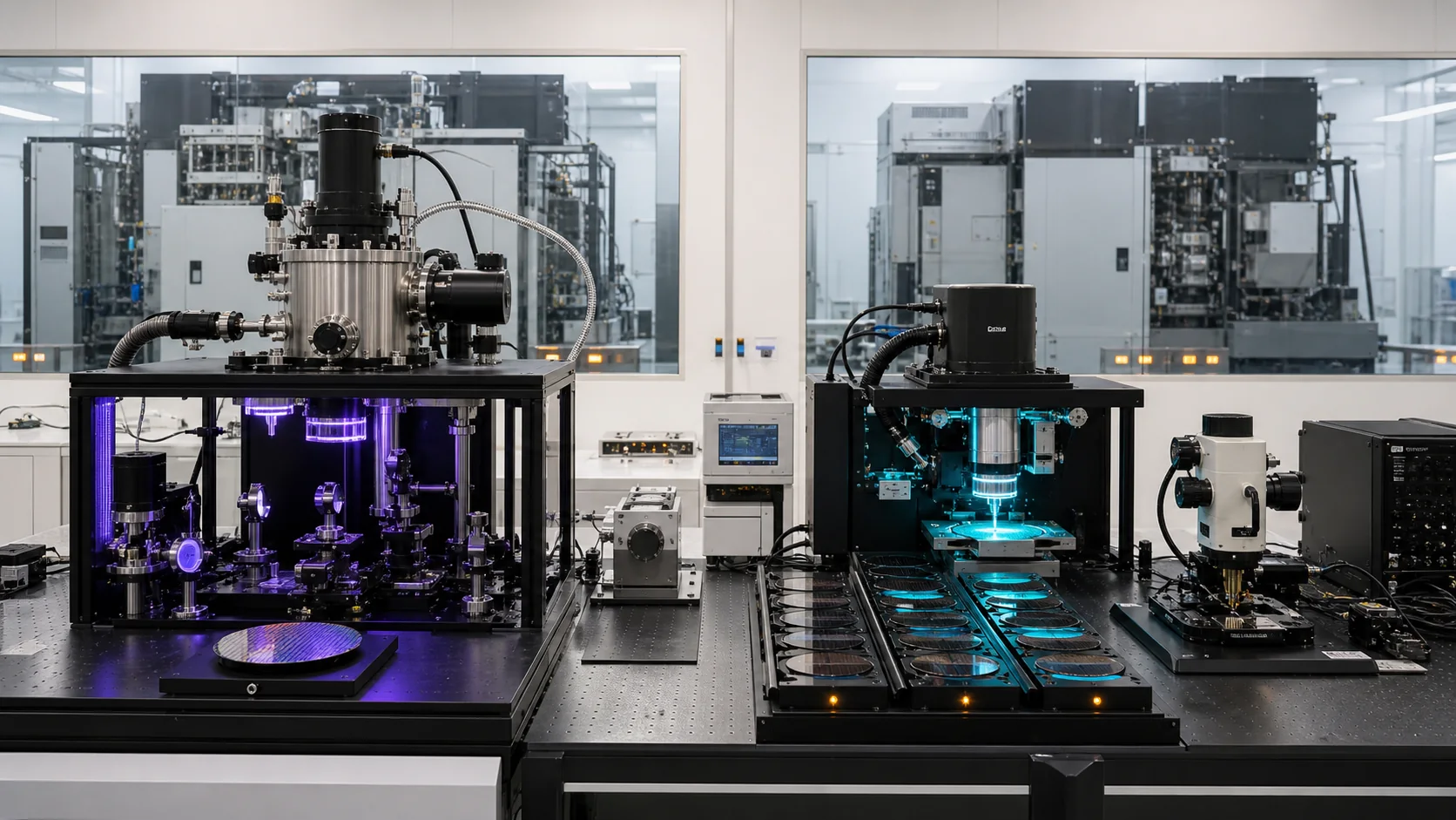
- full-angle aperiodic La/B-based reflectivity and phase;
- roughness PSD and image-flare propagation;
- phase-reticle fabrication, inspection, repair, cleaning, and lifetime;
- B-based pellicle transmission, strength, particles, and thermal survival;
- dense inorganic resist absorption, electron range, chemistry, outgassing, development, and transfer.
For E13:
- ERL-FEL power, bandwidth, pointing, polarization, coherence, uptime, and recovery;
- FEL-to-scanner transport and fast isolation;
- B1 imaging and thermal qualification at the dose ladder;
- B2 hyper-NA optical feasibility, 6x-or-higher mask format, vector imaging, and field performance.
Phase 2, microfield and alpha tools
- Q6 6.65 nm microfield imaging and electrical transfer loop.
- B1 source-coupled scanner demonstration that isolates source effects from current LPP behavior.
- B2 alpha imaging only after its optical model closes and Gate B supports an economic dose.
Phase 3, 300 mm integrated qualification
Exercise the real workflow:
- material deposition and underlayer;
- wafer measurement, chucking, topography, grid, and temperature mapping;
- reticle inspection and recipe release;
- exposure at selected dose and production scan order;
- post-exposure process and pattern transfer;
- e-beam plus electrical defect measurement;
- source interruption, beamline failover, restart after idle, and long-lot drift;
- matched-machine and source-path comparison;
- cost per good wafer on a real candidate layer.
Phase 4, HVM pilot
Advance only if the selected design demonstrates:
- required resolution and image slope;
- electrical defect tails with stated confidence;
- thermal overlay and focus within allocation;
- source and scanner availability with N+1 behavior;
- qualified masks, materials, inspection, cleaning, and supply;
- lower cost per good wafer than the incumbent flow.
Part VIII. Risk register and kill conditions
24. What kills or redirects Design A?
| Risk | Kill or pivot condition |
|---|---|
| Image slope | measured 6.65 nm aerial NILS below 2.53 against B2, unless cost and floor evidence still justify A |
| Coating | full-pupil reflectivity, phase, bandwidth, or lifetime misses the power and image budget |
| Roughness and flare | measured PSD-propagated flare consumes the contrast gain |
| Resist | no film meets absorption, response, blur, sensitivity, defect, outgassing, and transfer requirements together |
| Phase reticle | mask cannot be fabricated, inspected, repaired, cleaned, or kept stable at yield |
| Pellicle and particles | no pellicle or pellicle-free flow meets added-defect and lifetime limits |
| Source | 6.65 nm power, transport, uptime, redundancy, or coherence conditioning misses the selected dose and throughput |
| Economics | no product layer beats B2 or the incumbent cost per good wafer |
25. What kills or redirects Design B?
| Risk | Kill or pivot condition |
|---|---|
| Dose saturation | measured total sigma or electrical tails flatten above the product target |
| Hyper-NA optic | no feasible 0.75 NA optical design closes wavefront, mirror, polarization, field, and manufacturability budgets |
| Mask angular acceptance | real pupil and coating cannot support the required field and NILS at an economic demagnification |
| Depth of focus | 24 nm modeled DOF cannot support the resist, topography, flatness, and focus-error stack |
| Wafer and reticle heat | measured overlay, CD, or focus exceeds allocation at the economic dose |
| FEL coherence, shared with Design A | residual speckle or standing waves consume CDU or stochastic margin |
| Shared-source availability | source or beamline failure cannot preserve fleet output and unambiguous wafer state |
| Field overhead | smaller B2 field prevents useful throughput even with sufficient power |
| Economics | source share, hyper-NA capital, cooling, downtime, and yield do not beat Q6 or the incumbent flow |
FEL coherence is a common-mode risk because Design A draws on the same source class. One image-plane speckle-decorrelation gate should test both designs, and the result does not favor either wavelength by itself.
Part IX. What is proven and what is not?
26. What evidence exists today?
Evidence exists for individual pieces:
- tabulated atomic optical constants;
- a measured 64.1% La/B-based periodic coupon at 6.65 nm;
- early beyond-EUV zinc-containing resist response;
- current 0.55 NA High-NA imaging and electrical-yield work;
- ERL and FEL mechanisms and a detailed 10 kW-class 13.5 nm design;
- EUV wafer and reticle thermal-deformation mechanisms;
- 13.5 nm coatings, masks, resist families, pellicles, inspection, and contamination practice.
27. What remains unproven?
- No integrated 6.65 nm scanner exists.
- No full-angle Q6 coating meets the complete pupil, bandwidth, phase, heat, contamination, and lifetime requirements.
- No 6.65 nm phase reticle has demonstrated NILS 2.53 across a useful process window.
- No dense 6.65 nm resist has demonstrated the required absorption, chemistry, blur, dose, defects, dry development, and transfer together.
- No Q6 pellicle and actinic mask-inspection ecosystem is qualified.
- No 0.75 NA B2 projection optic exists.
- B2's assumed aerial NILS 2.0 has not been simulated or measured at its real mask angles and polarization.
- The 6x slit conclusion is a first-order angular-bandwidth estimate, not a full optical design.
- No ERL-FEL runs at semiconductor fab duty or feeds a redundant scanner fleet.
- No measured High-NA dose ladder has yet supplied the non-photon floor required by this decision model. Published comparative dose-scaling work exists: the accessible abstract for Bhattarai, Neureuther, and Naulleau describes matched-image-slope LER experiments under EUV and electron-beam exposure at 50 nm half-pitch. Search-surfaced summaries also attribute a dose-to-the-minus-one-half fit with high correlation to the paper, which would favor Design B, but neither agent could verify that fit or its numerical coefficients from the inaccessible full text. The claim is therefore recorded but not used as evidence, and the experiment does not replace Gate B at High-NA and 100 to 400 mJ/cm2. Bhattarai et al., JVST B 35, 061602
- Neither design has demonstrated its thermal, overlay, throughput, restart, persistence, and electrical-yield workflow end to end.
- Neither design has a measured cost per good wafer.
The study verifies arithmetic, internal consistency, source interpretation, and comparative logic. It does not verify the underlying physical performance of an unbuilt machine.
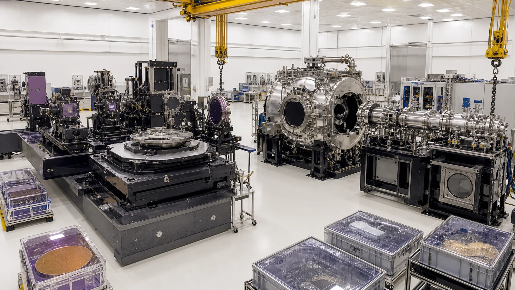
Part X. Final recommendation
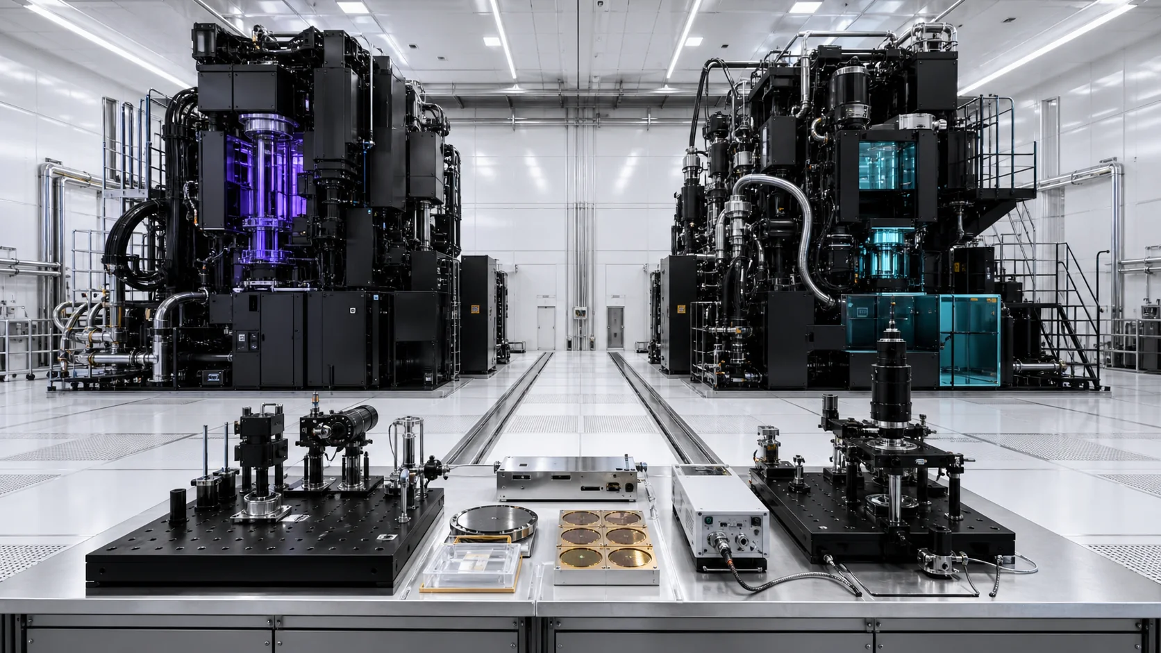
28. Which machine should be funded?
Fund the discriminating experiments before the production machines.
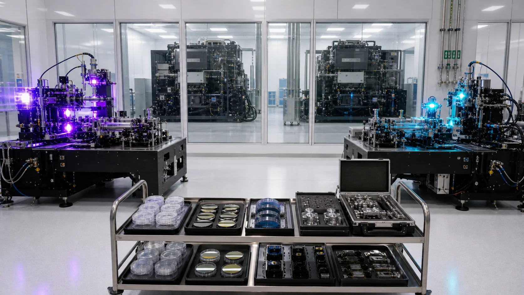
- Run the High-NA dose ladder and electrical-tail programme first. It tells us whether abundance has a ceiling.
- In parallel, measure 6.65 nm dense-film absorption and response, then simulate the phase-reticle image slope.
- If the dose floor is low, pursue E13 B1 immediately as the transition platform and B2 as the 6 nm end-state, subject to hyper-NA feasibility.
- If the dose floor is material and Q6 NILS clears 2.53, pursue Q6 because contrast and process-noise deletion become necessary rather than optional.
- If both paths remain viable, let measured cost per good wafer decide layer by layer. A fab may ultimately use both: B1 for mature high-yield 8 nm work and Q6 or B2 for the layers that truly require 6 nm half-pitch.
29. Final verdict
The first report produced a strong 6.65 nm contrast machine. The second concept exposed the unpriced alternative: keep 13.5 nm and make photons abundant. Building both designs on one model produced the more useful answer.
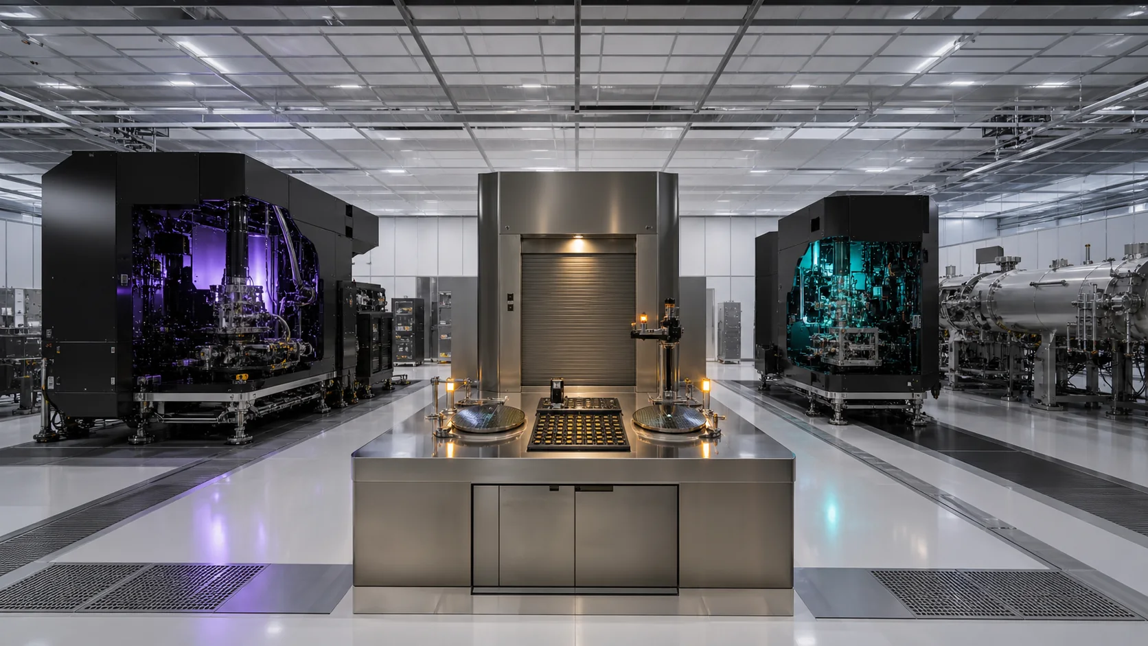
Q6 Sentinel is the higher-contrast, lower-dose, larger-DOF 6 nm route, with severe new-material and coating risk. E13 Photon Foundry is the established-wavelength route, with a lower-risk 8 nm bridge and a credible but unbuilt hyper-NA 6 nm branch, carrying severe optical, field, thermal, and noise-floor risk.
Neither defeats quantum randomness. Each changes how much that randomness matters. Q6 makes every absorbed photon more effective through contrast and a redesigned process stack. E13 tries to make photons cheap enough that the square-root penalty recedes. The correct choice depends on whether real process error continues to fall with dose and whether a 6.65 nm phase system can deliver its modeled image slope.
Those are measurable questions. That is why the report ends with two gates, not a promise.
Appendix A. Reproducible core values
A.1 Shared stochastic model
absorptance = 1 - exp(-mu * thickness)
blur_MTF = exp(-2 * pi^2 * blur_sigma^2 / pitch^2)
NILS_eff = NILS_aerial * blur_MTF
A_corr = 2 * pi * blur_sigma^2
N_corr = absorbed_photons_per_nm2 * A_corr
sigma_EPE = CD / (NILS_eff * sqrt(N_corr))
Shared comparison assumptions: 20 nm film, 1.5 nm blur sigma, pitch equal to twice half-pitch, 15 per micrometre absorptance coefficient for the 13.5 nm tin-containing model branch, 20 per micrometre for the 6.65 nm Zn-rich design branch.
A.2 Key optical and stochastic values
Q6 k1 = 6 * 0.45 / 6.65 = 0.406015
B1 k1 = 8 * 0.55 / 13.5 = 0.325926
B2 k1 = 6 * 0.75 / 13.5 = 0.333333

Q6 DOF = 6.65 / 0.45^2 = 32.8395 nm
B1 DOF = 13.5 / 0.55^2 = 44.6281 nm
B2 DOF = 13.5 / 0.75^2 = 24.0000 nm

Q6 sigma at 40 mJ/cm2 = 0.2954 nm
B1 sigma at 40 mJ/cm2 = 0.4767 nm
B2 sigma at 40 mJ/cm2 = 0.4092 nm

B1 parity dose = 40 * (0.4767 / 0.2954)^2 = 104.18 mJ/cm2, unrounded model
B2 parity dose = 40 * (0.4092 / 0.2954)^2 = 76.76 mJ/cm2, unrounded model
A.3 Field-aware throughput model
WPH = 3600 * productivity_derating
      / (wafer_energy / usable_wafer_power
         + field_count * field_turnaround
         + swap_and_calibration)
Assumptions: productivity derating 0.85, field turnaround 0.040 s, swap and calibration 4.5 s, 170 fields for A and B1, 255 fields for B2, 650 cm2 patterned area.
At 150 WPH:
available raw wafer time = 3600 * 0.85 / 150 = 20.4 s
A and B1 exposure window = 20.4 - 170 * 0.040 - 4.5 = 9.1 s
B2 exposure window = 20.4 - 255 * 0.040 - 4.5 = 5.7 s
A.4 Verification evidence
- Claude's
two_designs_model.pyreproduced the first report's 0.4767 and 0.2954 nm regression values before calculating B1 and B2. - Codex independently reimplemented the formulas in PowerShell and reproduced B1 and B2 parity, DOF, NILS crossover, Bragg-spread estimates, field count, and field-aware fanout.
- The model's regression check was deliberately broken by doubling sigma. Codex's audit showed that it printed
regression: FAILand still exited 0, making it a diagnostic rather than a test. Claude hardened the guard so a failed check now aborts with exit code 1 and prints no report body. Re-tested after the change, the perturbed model exits 1, while the restored model exits 0 and reproduces its committed output byte-for-byte. - One stale generated-output line, 3.2% versus executable 3.3% six-mirror scatter, was found. Claude regenerated the output. Codex reran the final model and confirmed exact equality over 365 normalized lines.
Appendix B. Primary source ledger
| Source | Used for | Boundary |
|---|---|---|
| IEEE IRDS 2024 Lithography and Patterning | High-NA and hyper-NA challenges, 6 to 7 nm platform change, equal-shot-noise dose penalty, FEL utility concept, polarization and infrastructure | roadmap and projection, not a demonstrated machine |
| CXRO atomic scattering factors | material optical constants and absorption-edge reasoning | isolated-atom tables; solid films near edges must be measured |
| Kuznetsov et al., 64.1% at 6.65 nm | La/B-based coating evidence | periodic coupon near normal incidence, not full-pupil scanner performance |
| Waltz et al., Zn-imidazolate EUV and beyond-EUV resist | first relevant 6.7 nm resist response and ALD/MLD film path | early material result, not Q6 production resist performance |
| Konomi et al., ERL-FEL cavity design | 800 MeV, 9.75 mA, 60 pC, 162.5 MHz, 10 kW-class 13.5 nm design basis | design and cavity analysis, not a delivered fab source |
| ASML EXE:5200B | 0.55 NA, 8 nm resolution, contrast, 50 mJ/cm2 throughput basis | commercial platform anchor, not an FEL or hyper-NA result |
| ASML 2025 annual report | industry-published 175 WPH EXE:5200B figure | published figure, not independently measured by the agents |
| Ronse, projection-lithography scaling review | typical dose range, stochastic contributors, High-NA process context | review evidence, not a 6 nm process demonstration |
| Bhattarai, Neureuther, and Naulleau, comparative shot-noise study | existence and abstracted scope of matched-image-slope EUV and electron-beam LER experiments | full text and search-surfaced fit coefficients were not accessible to either agent, so the claimed fit is recorded but excluded from the evidence base |
| imec High-NA electrical yield | end-to-end e-beam plus electrical validation pattern | 20 nm pitch test structures, not 6 nm half-pitch or extreme-tail proof |
| Chang, Engelstad, and Lovell | wafer heating mechanism and chuck sensitivity | finite-element analysis |
| Ko et al. | scan-dependent thermal deformation mechanism | modeled EUV die, not either proposed machine |
| Huddleston et al. | reticle thermal behavior above 500 W source class | current EUV reticle study, not direct Q6 or FEL qualification |
Appendix C. Collaboration and cross-verification record
Claude Code and Codex worked across both designs rather than assigning one machine to each peer.
- Claude Code: unified photon, stochastic, source, angular-bandwidth, flare, B1, B2, and decision-gate model.
- Codex: wafer and reticle thermal analysis, field-aware throughput, source fanout, cost-per-good-wafer framework, risk carry-over, development sequence, and final assembly.
Each peer opened and independently checked the other's material files. The cross-review found and closed real gaps:
- Codex's false conclusion that A alone reaches 6 nm.
- Claude's field-unaware 9.1-scanner B2 fanout.
- A stale generated-output line.
- Overbroad “qualified parts” and “near-zero physics risk” language for B2.
- Ambiguous replacement of the 2.17 NILS benchmark with 2.53 instead of naming both comparisons.
The combined result is stronger because neither peer's first conclusion survived unchanged.
Prepared under the Nexus Co-Lab collaboration contract. The human operator is the sole leader. Claude Code and Codex contributed as equal collaborators.