What is being proposed?
A 12-year program that starts with a 96-physical-qubit prototype and targets a modular machine with 1.31 million physical qubits and about 1,500 logical qubits.

Quantum computing research
From 96 physical qubits to a 1.31-million-qubit fault-tolerant system
A checkable technical plan connecting device physics, error correction, cryogenics, control, software, cost, and proof into one 12-year engineering program.
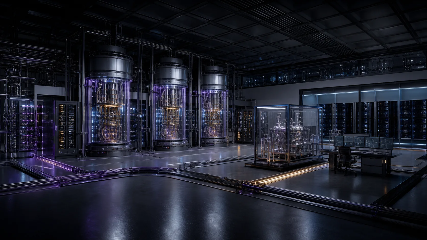
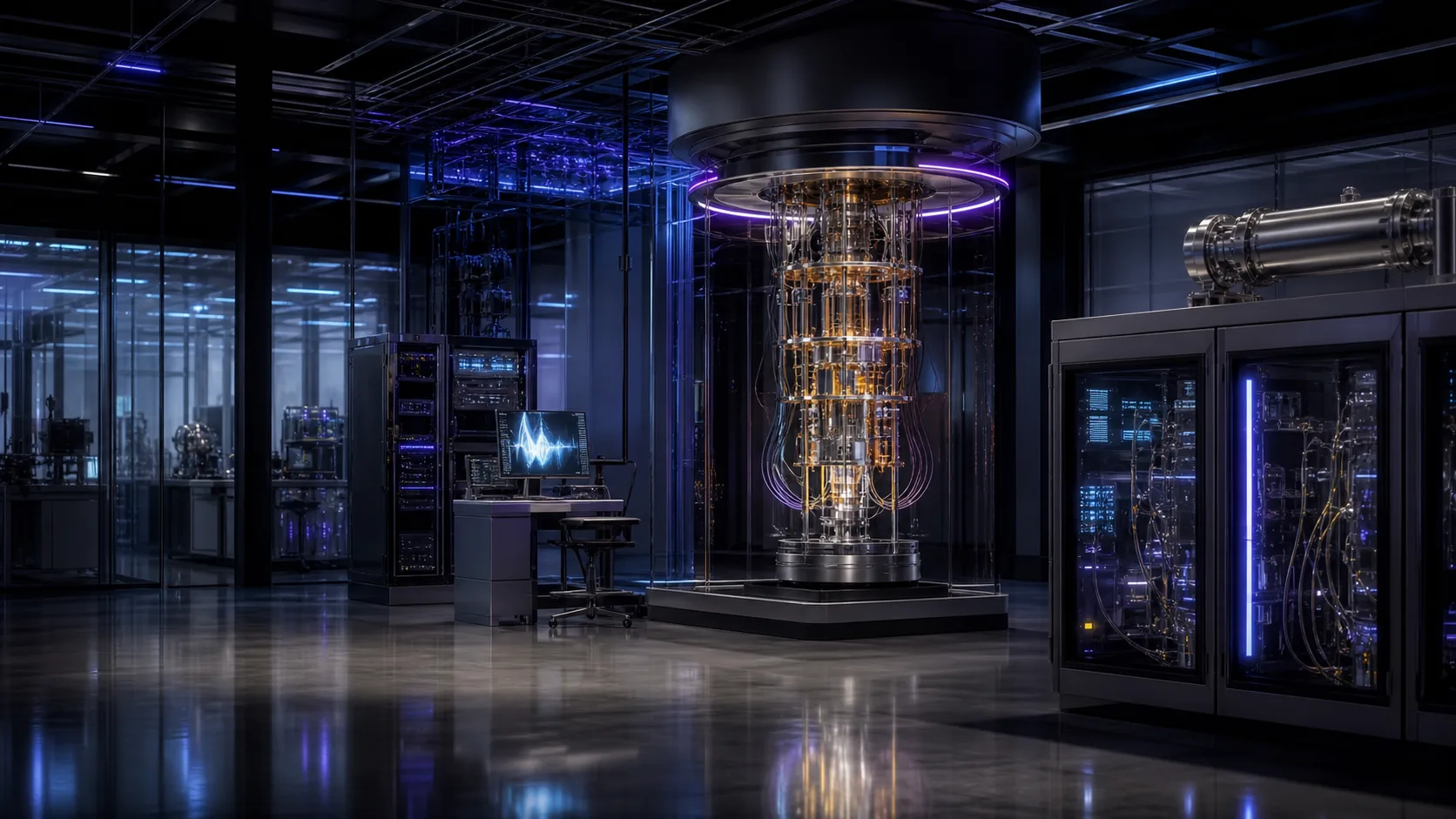
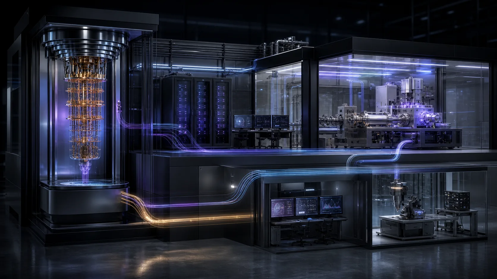
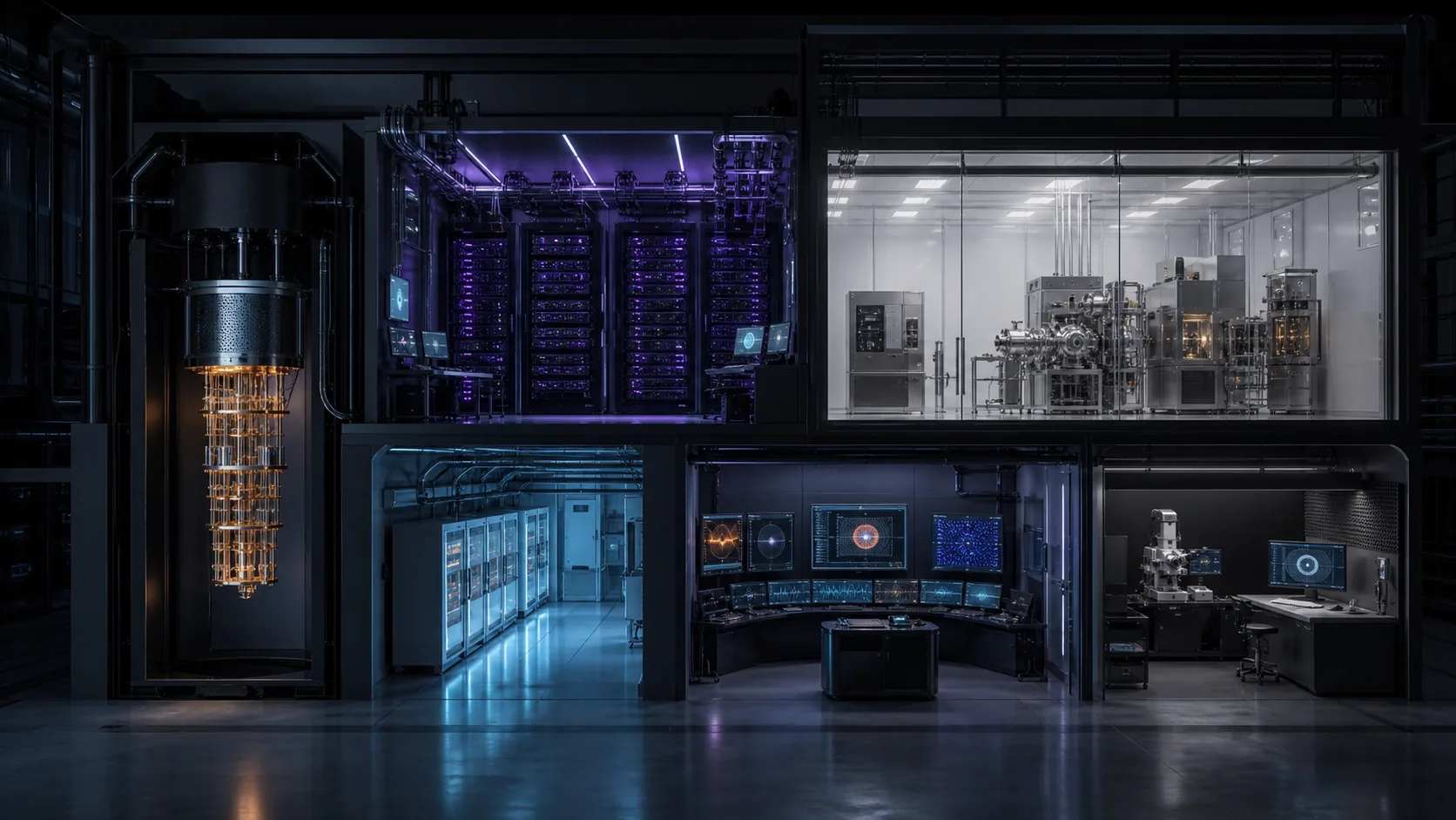
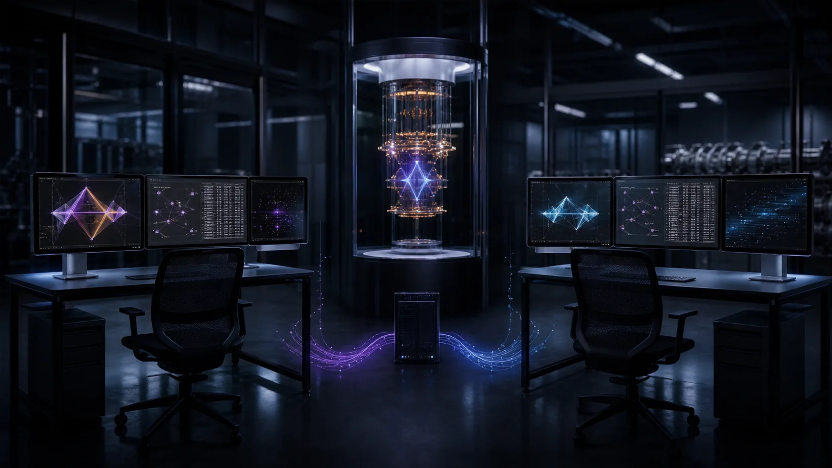
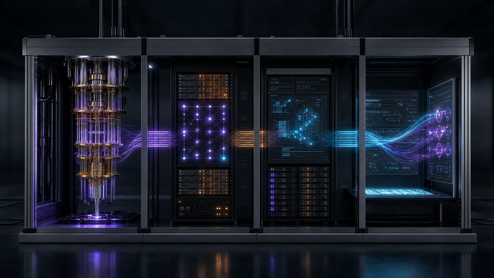
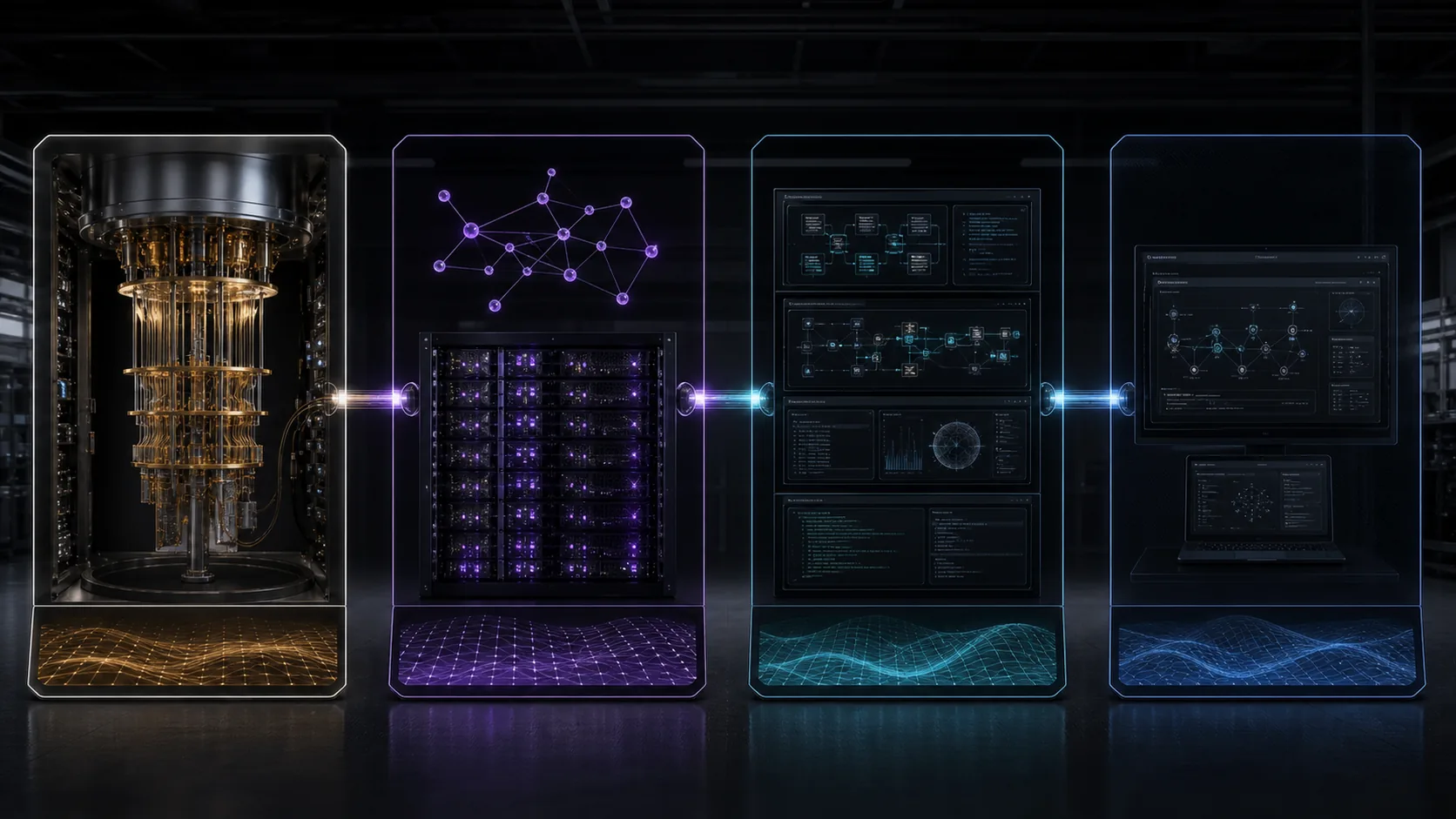
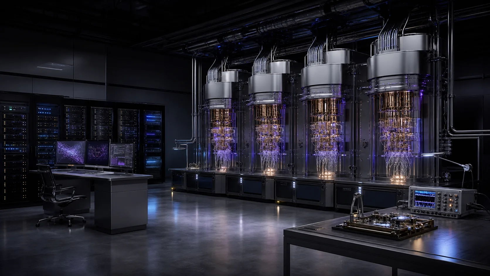
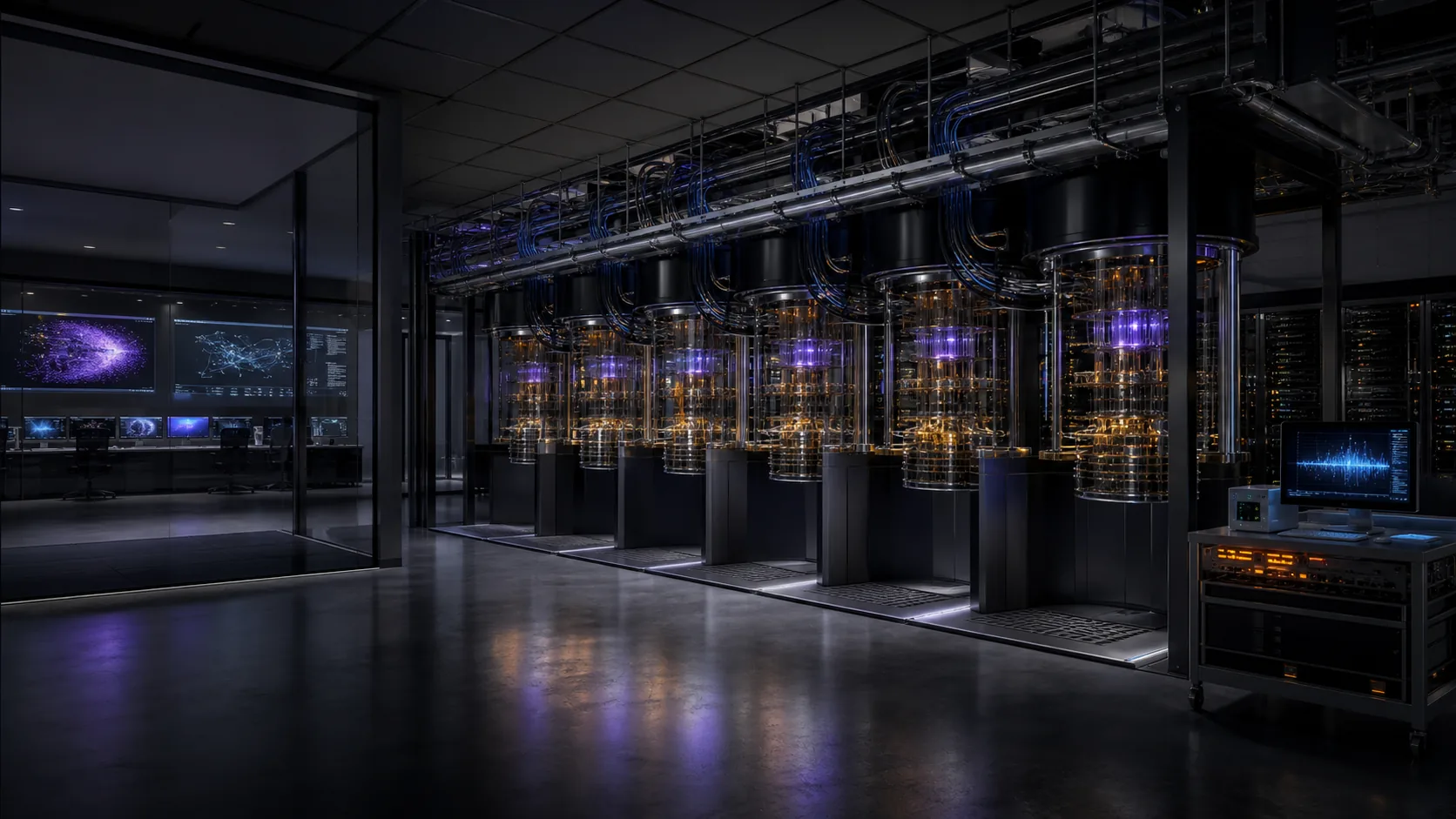
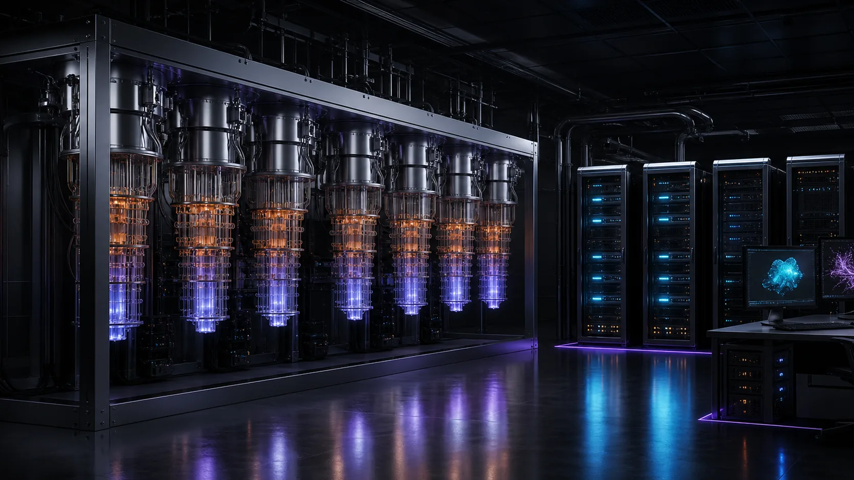
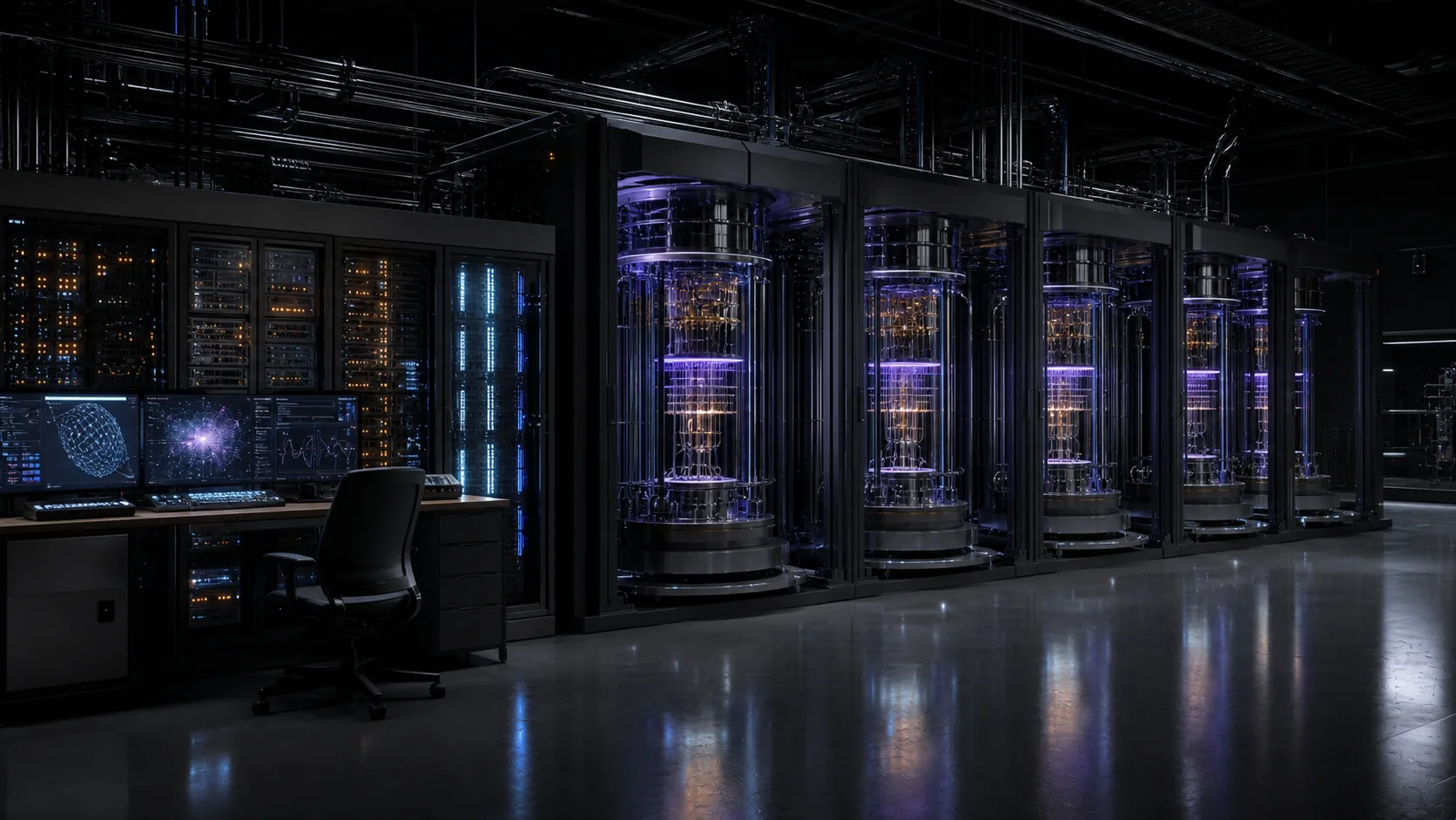
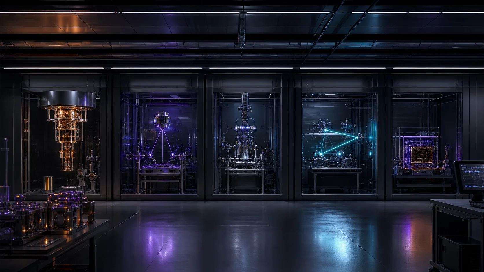
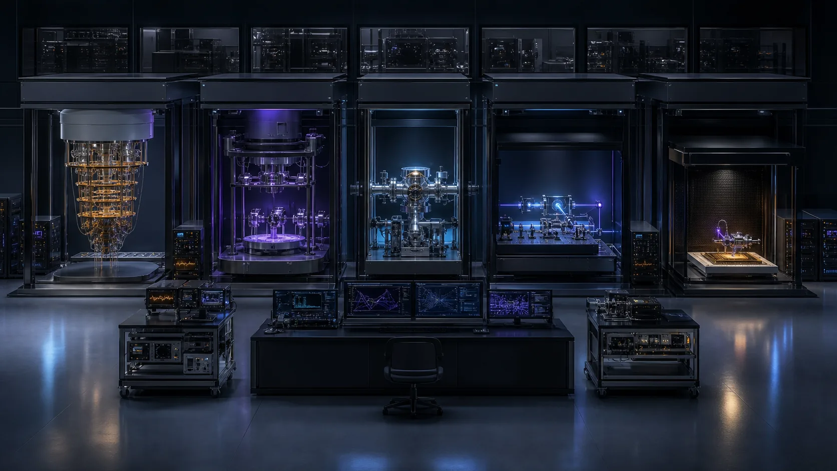
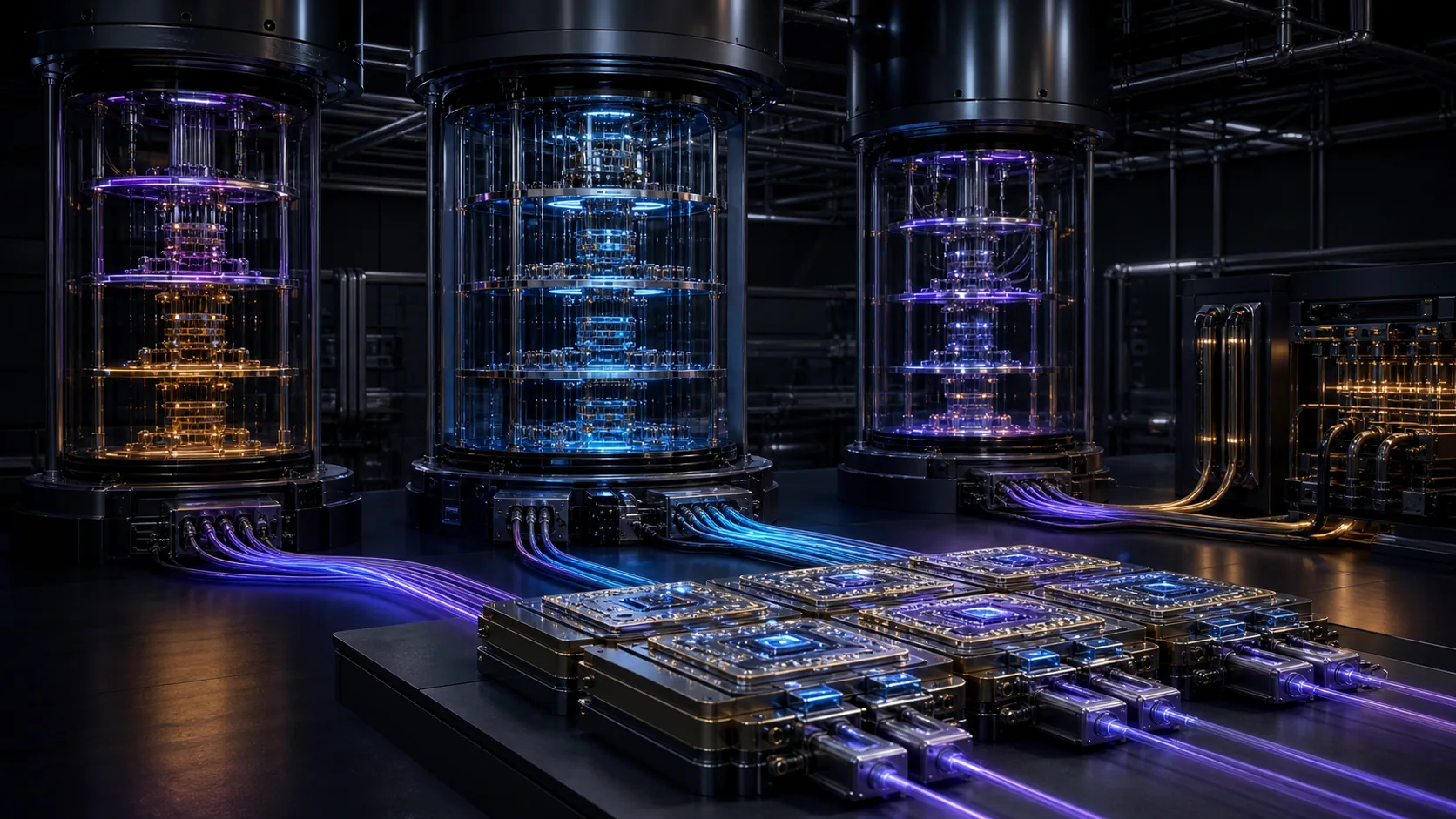
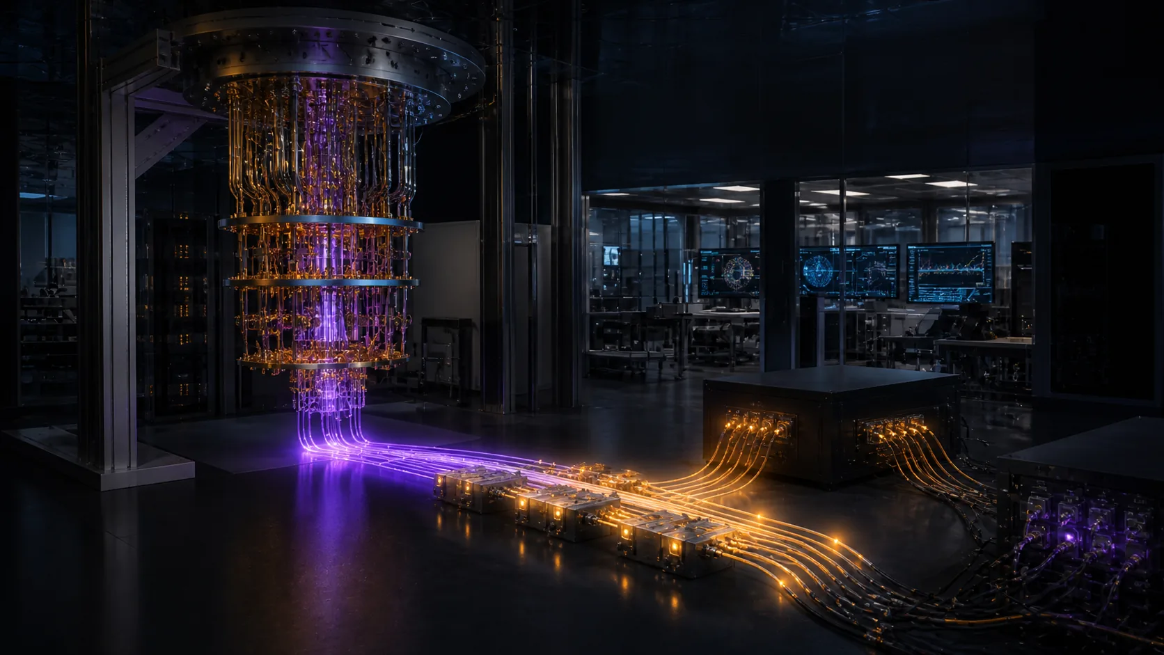
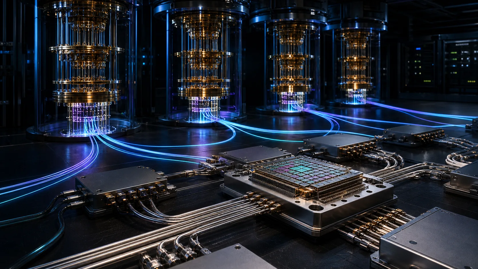
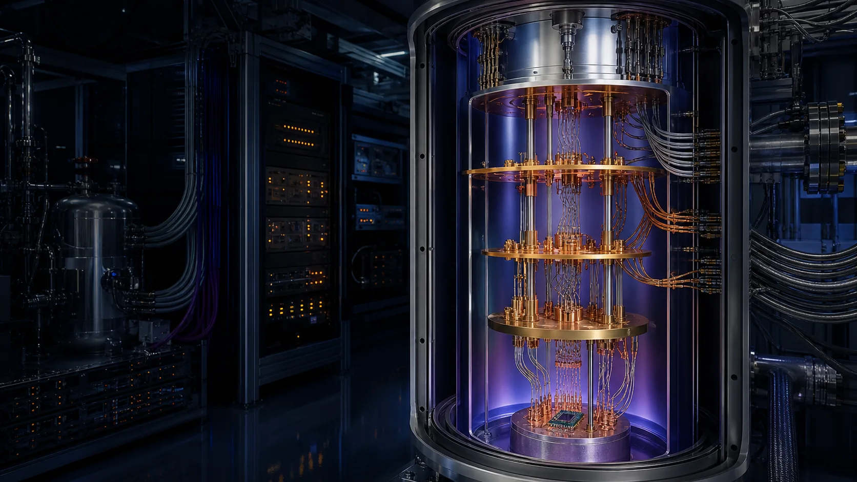
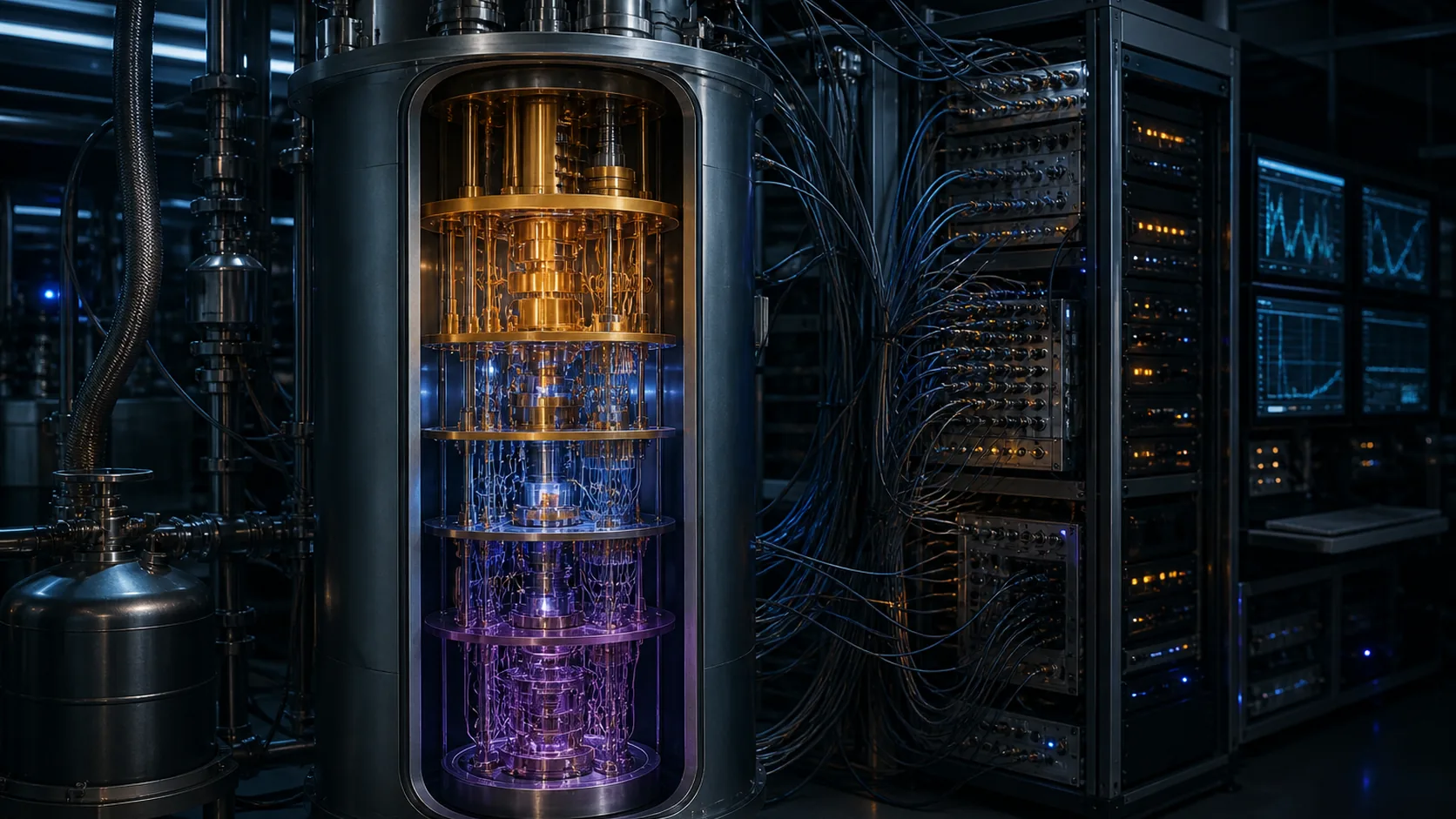
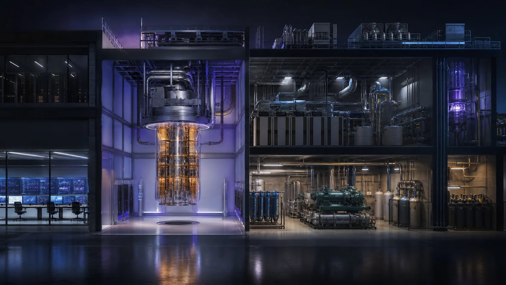
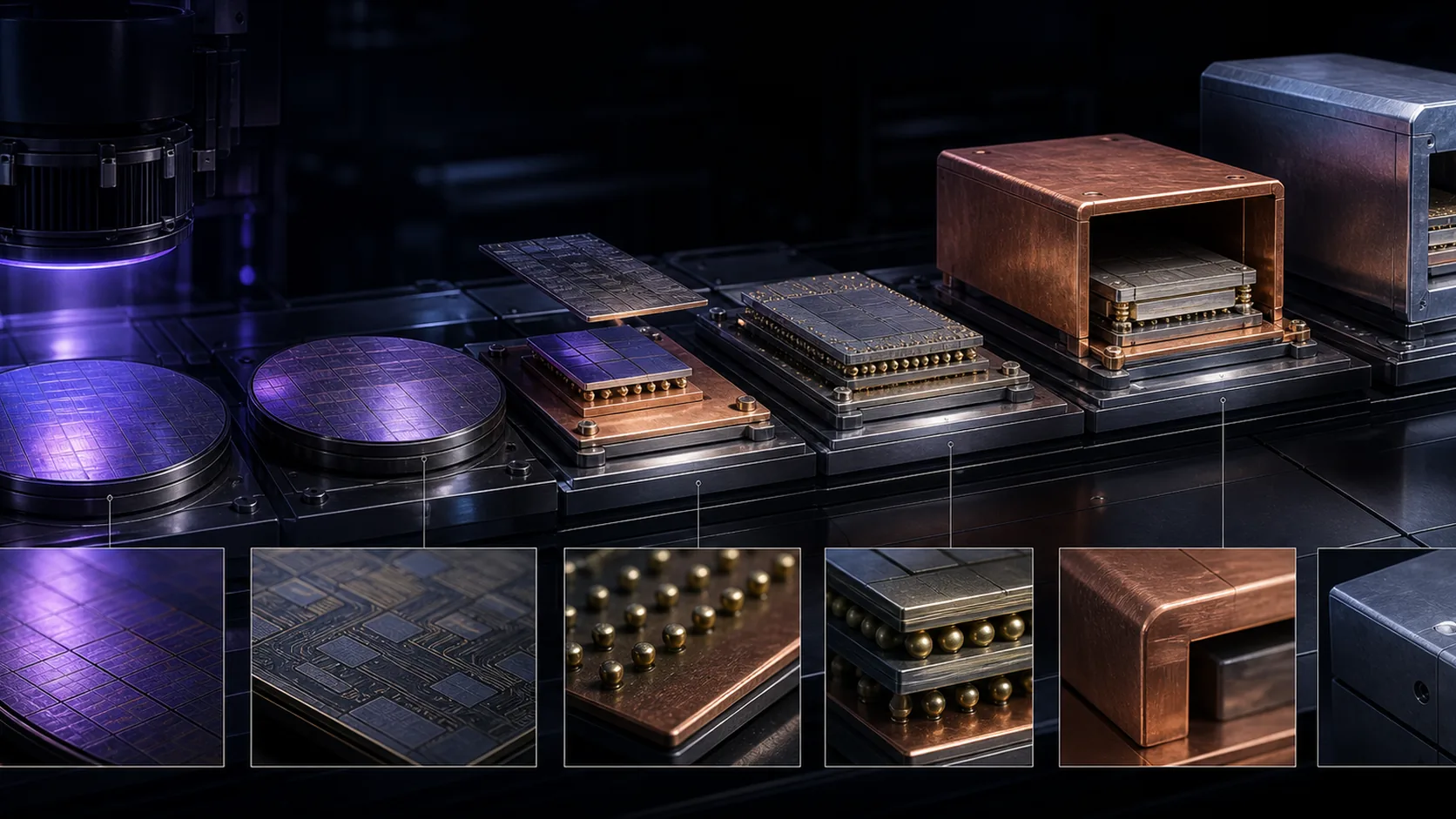
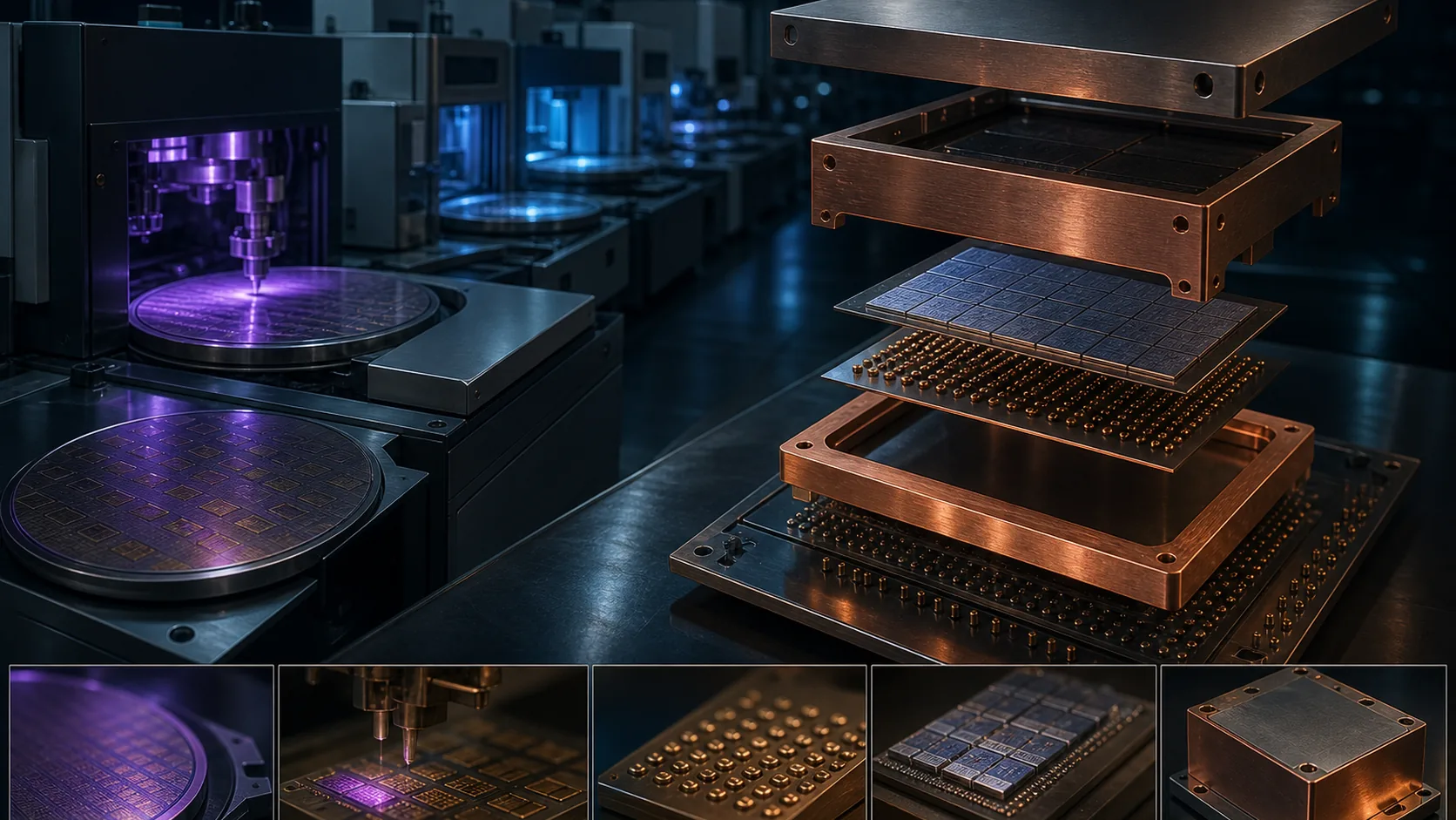
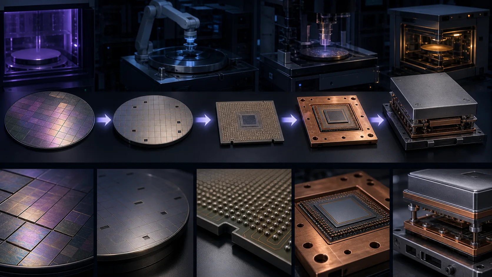
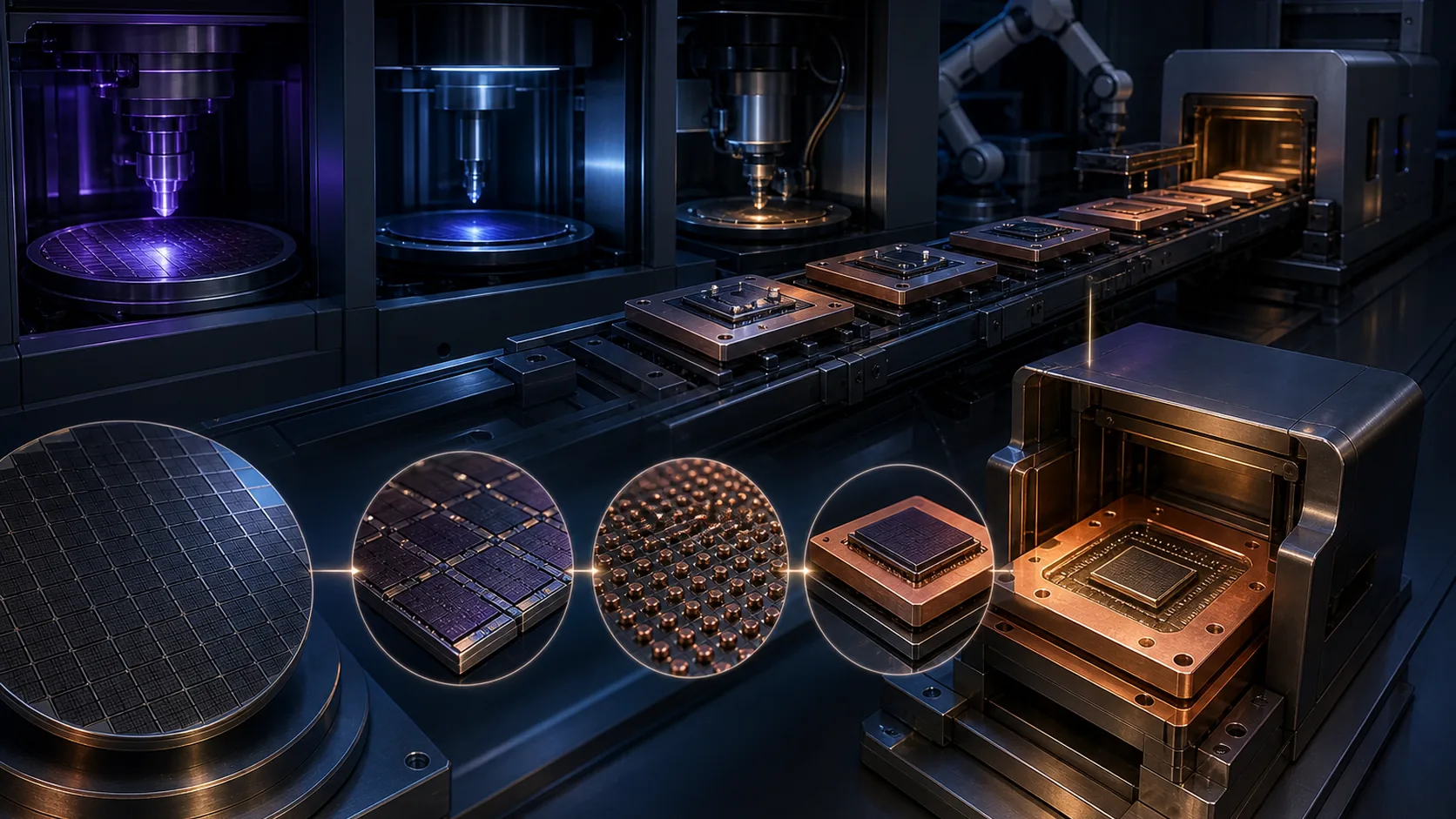
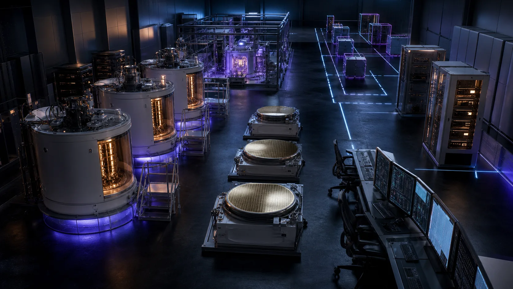
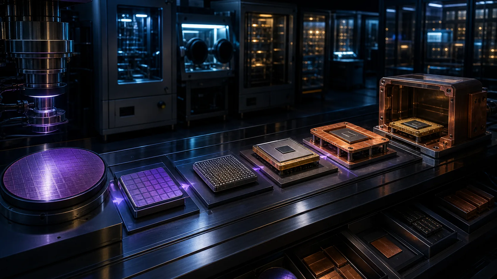
Status: No quantum hardware has been built or measured for this plan. Values marked source, estimate, or assumption retain those evidence boundaries. The images are editorial concepts, not photographs of completed machinery.
Direct answers
A 12-year program that starts with a 96-physical-qubit prototype and targets a modular machine with 1.31 million physical qubits and about 1,500 logical qubits.
CRY-1, the cryogenic wiring and control problem. The program cannot scale if control electronics, interconnects, heat load, and real-time feedback do not work together.
The plan gives superconducting hardware a narrow score advantage, 385 to 380, because its roughly 1 microsecond cycle supports faster error-correction feedback. Neutral atoms remain the explicit fallback.
The plan identifies three first-order unknowns: 4 K control power, distributed-topology overhead, and a 10 microsecond reaction target compared with a cited 63 microsecond measured result.
Read this first
This plain-language guide explains the terms used in the preserved technical plan. It does not change the plan's calculations, evidence tags, assumptions, open risks, or acceptance gates.
Definitions checked against primary or official sources: Google Quantum AI, quantum error correction below threshold, Bravyi et al., bivariate bicycle quantum memory, Gidney, fault-tolerant RSA-2048 resource estimate, Lee et al., fault-tolerant FeMoco resource estimate, Gidney, Shutty, and Jones, magic-state cultivation, Higgott and Gidney, Sparse Blossom decoder, Bluefors KIDE cryogenic platform, OpenQASM 3 specification, QIR Alliance, Gidney, Stim stabilizer circuit simulator, Magesan, Gambetta, and Emerson, randomized benchmarking, Erhard et al., cycle benchmarking. The wording is simplified for this article; the preserved report remains the authority for calculations, assumptions, and evidence boundaries.
A twelve-year program to build a machine that finishes a useful computation.
| Prepared by | Claude Code and Codex, Nexus Co-Lab, as equal 50/50 collaborators |
| For | Claudiu (Founder Nexus co-lab) |
| Date | 15 August 2026 |
| Status | Both parts written independently. Both cross-review passes complete: each author re-derived the other's arithmetic and challenged the other's assumptions, and both parts were revised as a result. |
| Part A, physical layer | Claude Code |
| Part B, logical layer | Codex |
| Assembly | Claude Code, at Codex's request. Neither author edited the other's part file. |
Every number in this plan is tagged. [SRC] is a cited public source. [EST] is arithmetic performed here on top of cited inputs, with the derivation shown. [ASM] is a design assumption we chose, not something measured.
The arithmetic is machine-checkable. Two scripts re-derive the numeric claims from their cited inputs:
verify/part-a-arithmetic-check.py     108 assertions, 0 failing
verify/part-b-arithmetic-check.py      28 assertions, 0 failing
assembly/assemble.py                   rebuilds this document and re-checks its integrity
Each was written by the author of the other part where possible. Part B's checker in particular recomputes from Codex's sources rather than reading his stated results, which is the only way a check means anything.
Run them:
python verify/part-a-arithmetic-check.py
python verify/part-b-arithmetic-check.pyA fault-tolerant, gate-based, superconducting quantum computer of roughly 1.31 million physical qubits yielding on the order of 1,500 logical qubits, delivered in four phases over about twelve years, at a Phase 3 capital cost of $1.8B low, $2.6B base, $6.1B high, with programme capital of $2.2B to $6.5B and about $1.3B of operating cost. [EST]
That spread is not padding. It is driven almost entirely by one unresolved number in a cryogenic control-electronics power budget (see finding 2), and naming it is more useful than averaging it away.
The acceptance criterion is deliberately not a qubit count. It is a finished computation whose answer can be checked: an exactly verifiable fault-tolerant workflow first, then RSA-2048, then chemistry beyond classical reach. A result no classical computer can reproduce is a result nobody can check, so it proves the machine works only after the checkable ones have passed.
1. The binding constraint is wiring, not qubits.
At today's practice of roughly 2.1 cryogenic signal paths per qubit, a million-qubit machine needs 2,520,000 coaxial paths [EST]. At the best available wiring density, 256 channels per cryostat side-loader [SRC], that is 9,844 side-loader ports. No cryostat geometry exists in which that is buildable. The same arithmetic in thermal terms: at the ~3 uW per qubit at 100 mK implied by commercial cryostat capacity [EST], the machine needs 3.6 W of cooling at 100 mK, which is 1,200 top-end dilution refrigerators, about $9 billion in refrigerators alone before a single qubit is fabricated.
The entire hardware plan is therefore organized around one requirement, CRY-1: get to 100 physical qubits per feedthrough and 0.05 uW per qubit, a 210x wiring and 60x thermal improvement, via multiplexing, then cryo-CMOS control at 4 K, then photonic links. If CRY-1 fails, the correct move is to switch modality to neutral atoms, not to build 200 refrigerators. That trigger is written down in advance in A2.4 so it cannot be rationalized away later.
2. This is a semiconductor and control-electronics program, not a physics program.
At Phase 3 scale the cost shape inverts against intuition [EST]:
| Share of Phase 3 capital | |
|---|---|
| QPU modules, the actual qubits | 7 percent |
| Dilution refrigerators | 6 percent |
| Fab line, control ASICs, facility | 40 percent |
| Full control and infrastructure block | 57 percent |
Cryogenics is 30 to 50 percent of capital at small scale [SRC] and becomes a rounding error at scale. Any org chart or vendor strategy that treats this as a physics effort with an engineering department attached will fail on cost before it fails on physics.
3. Clock speed decides the architecture, and the argument is weaker than it looks.
Both reference workloads are depth-limited, so runtime scales linearly with the error-correction cycle time. Scaling from the published sub-week RSA-2048 figure at a 1 us cycle [SRC]: at 100 us the same run takes about 2 years, at 1 ms about 19 years [EST]. That table is why the plan selects superconducting qubits.
The modality scores are 385 against 380 out of 500, a tie inside the noise of any scoring exercise, and the document says so rather than dressing it up. Neutral atom is carried as a live fallback with a written trigger.
Three separate findings then undercut the argument, and all three came from the second author reviewing the first:
withdrawn. It divided a low-distance qLDPC memory ratio by a distance-25 active surgery tile. The quantities are not commensurable, and the honest position is that neither modality's advantage has been converted into a like-for-like comparison** at equal workload and equal logical reliability.
nearest-neighbor grid [SRC]. This is a 20-cryostat machine joined by links, and it does not inherit that runtime. A distributed-overhead multiplier of only 1.41 consumes the entire margin to seven days, and nobody has measured it.
final-decoder latency at distance 5** [SRC], 6x over the entire 10 us reaction budget the architecture depends on.
Those are risks H15 and H13, tied with the wiring wall for the highest exposure in the plan. None is resolved. The modality decision therefore rests on less quantitative ground than a 385-to-380 score implies.
days with no modelled upper bound (A3.4).
published full-stack estimate [EST]. The original draft claimed otherwise; that claim was false. A Phase 4 is defined and priced at $3.8B incremental, and deliberately not baselined.
two published cryo-CMOS per-channel figures differ by 13.75x and straddle buildability: 3.1 W per cryostat is engineerable, 43.3 W is not (A5.4).
scale for the same hardware (A3.3).
justified (A3.1).
need 3e15 trials [EST], 95 years of continuous running at 1 us per trial.
quoted figures describe 5 to 20 qubit systems.
because the second author declined to invent figures that do not yet exist.
The two parts were written independently, then each author re-derived the other's numbers. This was not ceremony. It found:
changed a headline conclusion (the 7 percent qubit-cost finding above).
415), corrected by its author; the decision it supports is unchanged.
error quantities that differ by eight orders of magnitude.
figure and a decoder power figure, Codex declined to supply either, on the grounds that neither exists yet. Both are now explicitly bounded unknowns with defined closure gates instead of confident-looking estimates.
around a lost cryostat mid-job. It cannot: a logical state lives in specific physical qubits. Fixing this surfaced three hardware requirements neither part had captured, all currently unpriced.
Then the reverse pass, Codex's independent review of Part A, found 11 more (A10.1): a withdrawn runtime claim, a phase gate whose device was too small to run it, an uncosted cryogenic stage, an invalid headline comparison, a cryostat count 65.5x beyond vendor scale, a single-point cost estimate replaced by a $1.8B to $6.1B range, and 4 of the 5 highest-exposure risks in the register.
The arithmetic checker passed 73 of 73 throughout all of that, and now passes 108 of 108. It could not have caught any of those eleven, because each was a sound calculation resting on an unexamined premise. Checking the arithmetic and checking the premises are different jobs. This document needed both, and the second one required an author who had not written the thing being checked.
| Section | Contents | Author |
|---|---|---|
| A1 to A3 | Target spec, modality trade study, chip and module architecture | Claude Code |
| A4 to A7 | Cryogenics, the wiring wall, control and readout, fabrication, facility | Claude Code |
| A8 to A9 | Cost, schedule, staffing, hardware risk register | Claude Code |
| A10 to A12 | Open questions, cross-verification record, sources | Claude Code |
| B1 to B2 | Error model, error budget, QEC code selection | Codex |
| B3 to B5 | Decoder architecture, magic states, resource estimates | Codex |
| B6 to B7 | Software stack, verification and benchmarking | Codex |
| B8 to B9 | Software risk register, sources | Codex |
| Joint appendix | Agreed interface contract, open items, verification evidence | both |
Owner: Claude Code Status: corrected against Codex's Part B. Codex's independent review of Part A is outstanding; see A10 and A11.4 for what that leaves unverified. Companion part: part-b-logical-software.md (owner: Codex)
Evidence policy used throughout Part A: every hard number is tagged. [SRC] means taken from a cited public source. [EST] means an engineering estimate derived in this document from cited inputs, with the derivation shown. [ASM] means a design assumption chosen by us, not measured.
A fault-tolerant, universal, gate-based quantum computer whose acceptance criterion is a completed application run, not a qubit count. The machine is specified by the two workloads it must finish, because qubit count alone is a vanity metric that has already been revised by a factor of 20 in a single paper.
Reference workload 1, cryptanalytic. Factor a 2048 bit RSA integer. Gidney 2025 shows this needs fewer than 1 million noisy physical qubits and under one week of runtime, assuming a square nearest-neighbor grid, uniform 0.1 percent gate error, a 1 microsecond surface code cycle, and a 10 microsecond control system reaction time. [SRC] This is a 20x qubit reduction from the same author's 2019 estimate of roughly 20 million qubits and 8 hours. [SRC]
Reference workload 2, scientific. Compute the ground state energy of the FeMo cofactor of nitrogenase to chemical accuracy. Published estimates have moved from roughly 111 logical qubits and about 1e14 T gates (Reiher et al. 2017), to 2142 logical qubits and 5.3e9 Toffoli gates (Lee et al. 2021, roughly four days on 4 million physical qubits), to 1972 logical data qubits and 1.4e13 T gates for FeMoco-76 via double factorization qubitization, to roughly 1137 logical qubits and 3.4e8 logical T gates with spectral amplification. [SRC]
Both reference workloads are dominated by circuit depth, not by width. That makes the quantum error correction cycle time the single most architecture-defining parameter in this plan.
Derivation [EST]. Gidney's sub-week RSA-2048 runtime assumes a 1 microsecond QEC cycle. Runtime scales linearly with cycle time for a depth-limited circuit. Therefore:
| QEC cycle time | Representative modality | RSA-2048 runtime (scaled from < 1 week) |
|---|---|---|
| 1 us | superconducting | under 1 week [SRC] |
| 10 us | fast neutral atom (aspirational) | roughly 10 weeks [EST] |
| 100 us | neutral atom (plausible near term) | roughly 2 years [EST] |
| 1 ms | trapped ion with transport | roughly 19 years [EST] |
A machine that cannot finish the run inside a useful human timescale is not a machine, it is an experiment. This table is the reason the modality choice in A2 weights clock speed as heavily as it does, and it is the first thing Codex should attack if he disagrees.
| Parameter | Target | Basis |
|---|---|---|
| Physical qubits | 1.2 million | [EST] covers workload 1 with 46 percent margin. Does not cover workload 2; see A8.2 |
| Logical qubits at end of pipeline | approximately 1,500 | [EST] from A1.1 workloads |
| Physical two-qubit gate error | <= 1e-3, stretch 3e-4 | [SRC] Gidney assumption; 99.9 percent CZ already demonstrated |
| Single-qubit gate error | <= 1e-4 | [SRC] 99.994 percent demonstrated |
| Measurement plus reset error | <= 1e-3 per measured ancilla | corrected per Codex B1.2; see A11.2 |
| Measurement plus reset time | <= 600 ns | corrected per Codex B1.2; see A11.2 |
| QEC cycle time | 1 us | [SRC] Gidney assumption |
| Control reaction time (measure to feed-forward) | <= 10 us at p99.9 | [SRC] Gidney assumption, p99.9 qualifier from Codex B1.2 |
| Logical memory error per hot logical-qubit round | <= 1e-15 | corrected per Codex B1.2; extrapolated, not demonstrated |
| Non-Clifford resource error per consumed CCZ | <= 1e-12 | corrected per Codex B1.2 |
| Cultivated T-state error before 8T-to-CCZ | <= 1e-7 | corrected per Codex B4.1 |
| T1 | >= 200 us in-array, best-cell >= 1 ms | [SRC] 1.68 ms demonstrated in tantalum-on-silicon |
| Wall clock, RSA-2048 | unresolved, bounded below by 4.96 days | source assumes one square nearest-neighbor grid; this is a 20-cryostat machine. See A3.4 |
| Availability | >= 95 percent steady state | [ASM] aspiration; the 95 percent figure in the source describes small single-cryostat systems, not a 20-cryostat cluster |
Codex: A1.3 is my side of the interface contract. Your B1 should either accept these or send back the values your code choice actually needs, and I will rework A4 through A6 against yours.
Post-cross-verification note. Codex's B1.2 came back with tighter and better justified values on four rows, and the table above has been corrected to his. The important one is that my original draft listed a single "logical error rate per logical operation of 1e-9," which conflated three different quantities: logical memory error per round, non-Clifford resource error, and cultivated T-state error. They differ by eight orders of magnitude and they land on completely different parts of the hardware. That was my error, it is fixed above, and A11.2 records it. My original 5e-3 readout figure was also too loose by 5x.
Superconducting transmon. Google Willow, 105 qubits, December 2024: two below-threshold surface code memories, a distance-7 code and a distance-5 code with a real-time decoder, error suppression factor Lambda = 2.14 +/- 0.02 per distance-2 increase, 0.143 +/- 0.003 percent error per cycle on a 101-qubit distance-7 code, and 2.4 +/- 0.3 times beyond breakeven against its own best physical qubit. [SRC] IBM Nighthawk, 120 qubits, November 2025, and IBM Loon, an experimental processor integrating multi-layer on-chip routing, long-range c-couplers, and fast qubit reset as the testbed for its qLDPC scheme. [SRC] Materials: tantalum-on-silicon transmons at 1.68 ms coherence. [SRC]
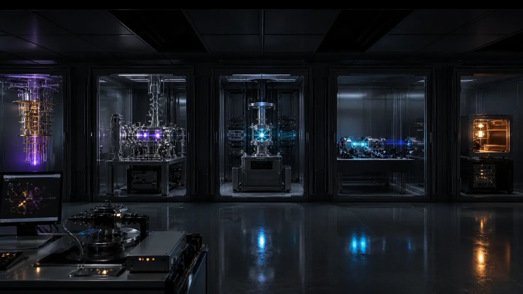
Trapped ion. Quantinuum Helios, 98 barium ions in a QCCD architecture, all-pairs two-qubit gate fidelity 99.921 percent, 48 error-corrected logical qubits from 98 physical. [SRC] Roadmap: Sol 2027, Apollo 2029 to 2030 with thousands of physical qubits and hundreds of logical qubits. [SRC]
Neutral atom. Harvard and MIT ran a 3,000-atom array continuously for more than two hours by reloading up to 300,000 atoms per second, defeating the atom loss lifetime that used to cap run duration. [SRC] QuEra and collaborators: 96 active distance-4 logical qubits on 448 physical atoms (Nature, November 2025), and a 2:1 physical-to-logical ratio using ultra-high-rate qLDPC codes in April 2026. [SRC]
Photonic. Room temperature optics, natural networking, but probabilistic entangling gates and severe loss budgets. No below-threshold logical memory demonstration comparable to the three above.
Spin in silicon. Best long-run CMOS foundry compatibility story of any modality, but qubit counts remain two to three orders of magnitude behind and two-qubit fidelity is not yet in the 99.9 percent class at array scale.
Weights chosen from A1.2: clock speed and fidelity dominate because our acceptance criterion is a finished application run.
| Criterion | Weight | Supercond. | Trapped ion | Neutral atom | Photonic | Si spin |
|---|---|---|---|---|---|---|
| QEC cycle speed | 20 | 5 | 1 | 2 | 4 | 4 |
| Two-qubit fidelity today | 20 | 4 | 5 | 4 | 2 | 3 |
| Demonstrated path to 1e6 physical | 20 | 4 | 2 | 5 | 3 | 4 |
| Connectivity and code efficiency | 15 | 2 | 5 | 5 | 4 | 2 |
| Engineering maturity and supply chain | 15 | 5 | 4 | 3 | 2 | 2 |
| Operating cost and complexity | 10 | 2 | 4 | 4 | 4 | 3 |
| Weighted total (max 500) | 385 | 335 | 380 | 310 | 310 |
Primary modality: superconducting transmon, tantalum-on-silicon, tunable coupler, modular multi-chip.
Named fallback: neutral atom.
The scores are 385 against 380. That is a tie inside the noise of any scoring exercise, and we should say so plainly rather than dress up a 1.3 percent margin as a clear win. The decision is therefore not "superconducting is better." It is:
is set by physics and readout, not by engineering effort. A 1 us cycle is demonstrated. Neutral atom cycle time is currently limited by mid-circuit measurement and atom rearrangement, and no credible path to 1 us exists today.
efficiency. The size of that win is not currently quantifiable, and an earlier draft of this section overstated it.
That draft divided the neutral-atom 2:1 physical-to-logical ratio [SRC] by the 1,352:1 of a distance-25 active surface-code tile and called the result a 676x overhead advantage. Codex's cross-review rejected that comparison and he is right. The two ratios are not commensurable: the 2:1 figure is a low-distance qLDPC memory result, and 1,352:1 is an active lattice-surgery tile at mission distance. They differ in code distance, logical reliability, available logical gates, routing, factory overhead, and experimental maturity. Dividing them produces a number with no operational meaning, and it was the most misleading figure in the draft.
What can honestly be said: neutral atoms have demonstrated materially better code efficiency at the distances tested so far, and superconducting qubits have demonstrated materially better clock speed. Neither advantage has been converted into a like-for-like comparison, which would require the same workload at the same logical reliability, compared on total spacetime volume and energy. That comparison does not exist in this document and should be built before the fallback in A2.4 could ever displace the baseline.
Codex's B1.4 also corrects the tile figure itself: 2d^2 - 1 = 1,249 is the raw memory patch, while active lattice-surgery planning needs 2(d + 1)^2 = 1,352. I have adopted 1,352 throughout.
real trigger, defined in A2.4.
Switch the primary to neutral atom if, at the Phase 2 gate (A8), any two of:
feedthrough line, making the Phase 3 fridge count exceed 400.
error rate matching our A1.3 target.
by more than one order of magnitude.
Trapped ion is not a Phase 3 candidate under A1.2 arithmetic, but it is the best available platform for early logical algorithm development, and we should buy access rather than build it. See A8 Phase 0.
The unit of manufacture is a module, not a chip and not a fridge.
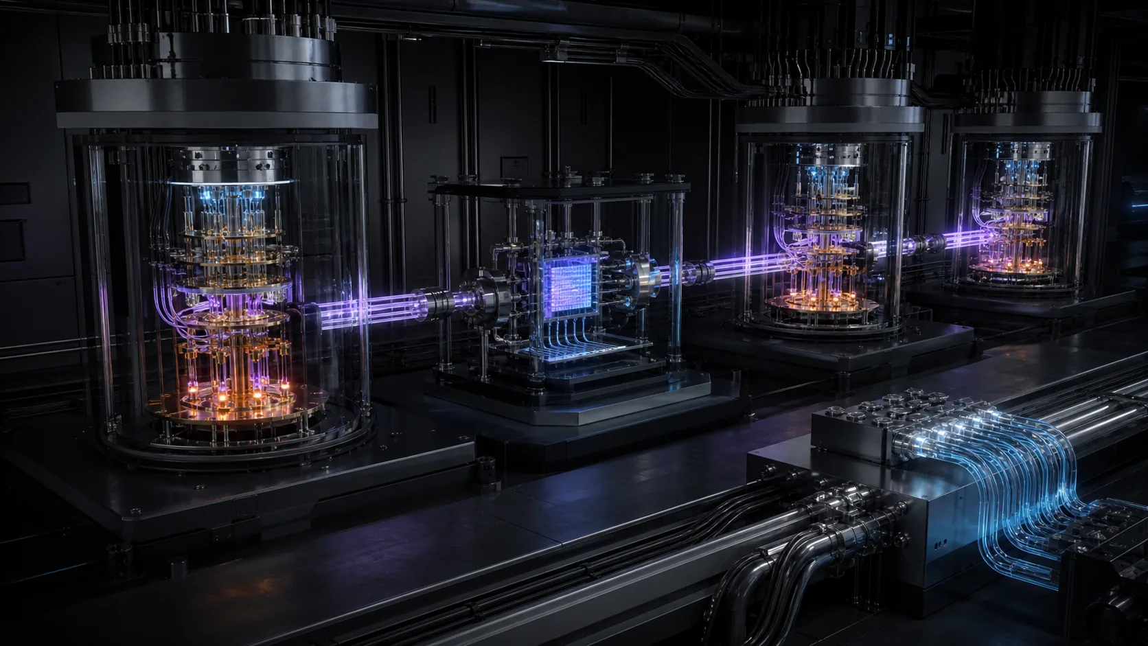
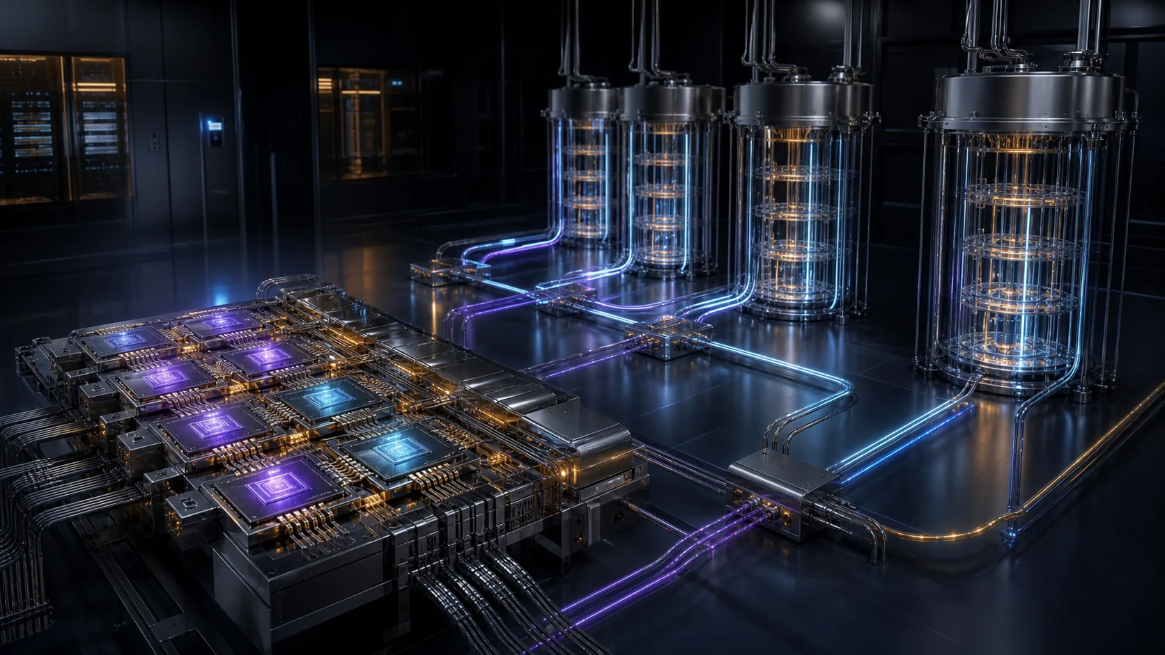
| Property | Value | Basis |
|---|---|---|
| Physical qubits per module | 1,024 data plus ancilla | [ASM] power of two for tiling and addressing |
| Lattice | square grid, nearest neighbor, tunable couplers | [SRC] matches Gidney's assumed topology |
| Die | tantalum base layer on high-resistivity silicon | [SRC] millisecond coherence platform |
| Stack | 3D integrated: qubit die bump-bonded to an interposer carrying routing and TSVs | [SRC] IBM Loon demonstrates multi-layer on-chip routing |
| Inter-module link | multi-chip tunable coupler and, for longer reach, microwave photonic link | [SRC] multichip tunable coupler demonstrated |
Module size is a gated design variable, not a fixed choice. [ASM]
The 1,024 figure came from a rationale that Codex's cross-review correctly took apart. The original argument was that since a distance-25 active tile needs 1,352 physical qubits, a 1,024-qubit module deliberately does not contain a whole logical qubit, which forces every logical patch across a module seam and so exercises the inter-module link from Phase 2 rather than discovering it is inadequate at Phase 3.
The half of that which is sound: integration risk should be pulled forward, not deferred. The half which is not: it dresses up a liability as a virtue. Putting a seam through every mission-distance logical patch means every logical operation in the machine depends on seam fidelity being equivalent to on-die fidelity, and no such equivalence has been demonstrated. If it fails, it fails everywhere at once, with no fallback layout.
Revised position:
margin**, so at least 1,352 physical qubits and preferably around 1,600, and the exact figure is set at the Phase 1 gate. [ASM]
forces seams, which is what makes it a good instrument for measuring them.
demonstrated seam equivalence: logical error rate for a patch spanning two modules statistically indistinguishable from the same patch on one die, at mission distance, under simultaneous operation.
Until that is measured, a seam-spanning mission layout is not baselined.
| Tier | Contents | Physical qubits |
|---|---|---|
| Module | 1 qubit die + interposer + carrier | 1,024 |
| Cluster | 8 modules on one cold stage, coupled by multi-chip couplers | 8,192 |
| Cryostat | 8 clusters (Phase 3 target, requires A5 to succeed) | 65,536 |
| System | 20 cryostats linked by microwave photonic interconnect | 1,310,720 |
The system tier at 1.31 million physical qubits covers the 1.2 million target of A1.3 with roughly 9 percent margin [EST].
The 65,536 qubits per cryostat figure in the table above is the single most aggressive claim in Part A, and the honest way to present it is against what the vendor actually publishes rather than against a vague sense of "commodity practice."
Bluefors KIDE published specification [SRC]:
| KIDE parameter | Vendor figure |
|---|---|
| Cooling power at 100 mK (across 3 sections) | > 3,000 uW |
| Cooling power at 20 mK (across 3 sections) | > 90 uW |
| Qubits supported | > 1,000 |
| RF lines supported | over 4,000 |
| Base temperature | 10 mK |
| Base flange size / max payload | 1.6 m^2 / 500 kg |
Set against the A3.2 system tier [EST]:
| Vendor scale, 20 KIDE | This plan | Extrapolation | |
|---|---|---|---|
| Qubits | 20,000 | 1,310,720 | 65.5x |
| RF lines available | 80,000 | 13,107 needed if CRY-1 holds | fits, with 6x margin |
| RF lines needed without CRY-1 | 80,000 | 2,752,512 | 34.4x over |
Two things follow, and they should be read together.
First, 20 KIDE-class cryostats support about 20,000 qubits at the vendor's published scale, not 1.31 million. This plan's cryostat tier is a 65.5x development extrapolation, not a procurement-ready configuration, and A8.3 prices it as though 20 units were sufficient. That is a stated assumption [ASM], not a quotation, and it is called out again in A11.4.
Second, and more usefully, the RF line rows show precisely what CRY-1 buys. At today's 2.1 paths per qubit the plan needs 34x more feedthroughs than 20 KIDE systems provide. At CRY-1's 0.01 paths per qubit it needs 13,107 lines against 80,000 available, which fits comfortably. The wiring wall is therefore not a vague scaling worry: it is the specific difference between a configuration that is 34x impossible and one that fits inside published vendor capacity.
The mixing-chamber row is the tightest constraint and was missing from the earlier draft. At > 90 uW at 20 mK per KIDE, a 65,536-qubit cryostat has a budget of about 1.4 nW per qubit at 20 mK [EST]. Nothing in this plan has been costed against that number, and it is a gap.
A5 is where these claims are earned or the plan collapses, and A5.5 states what happens if they are not.
This subsection exists because of Codex's cross-review, and it invalidates a headline claim the earlier draft made without qualification.
The problem. The RSA-2048 resource estimate this plan is sized against assumes a square grid of qubits with nearest neighbor connections, uniform 1e-3 gate error, a 1 us cycle, and a 10 us reaction time. [SRC] Those assumptions produce 897,864 physical qubits and 4.96 expected days. The A3.2 architecture is not a square nearest-neighbor grid. It is 1,280 modules, in 160 clusters, across 20 cryostats, joined by multi-chip couplers and microwave photonic links.
A distributed machine does not inherit a monolithic machine's resource count or runtime for free. Every logical operation whose lattice surgery crosses a link pays in extra rounds, extra ancilla, and extra failure probability, and none of that is in the 897,864 or the 4.96 days.
Consequence for this plan. The A1.3 wall-clock target of under 7 days and the Gate 3 RSA criterion are therefore not currently supported for the 20-cryostat topology. They are supported for the topology the source assumes, which we are not building. This is now labelled unresolved rather than baseline, and it is risk H15 in A9.
Requirement LNK-1, the link acceptance gate. [ASM] Before any distributed RSA runtime is baselined, every inter-module and inter-cryostat link class must have a measured budget for:
| Link property | Why it matters | Status |
|---|---|---|
| Logical error contribution per link operation | enters the failure budget in Codex's B1.3 | unmeasured |
| Link operation rate | sets how many surgeries can cross per cycle | unmeasured |
| Link latency | adds to the 10 us reaction budget of A5.3 | unmeasured |
| Link availability | a link outage is a partition, not a slowdown | unmeasured |
| Lattice-surgery overhead for crossing operations | the actual runtime multiplier | unmodelled |
The last row is the one that matters and it is the honest hole: we do not currently know the runtime multiplier for running this circuit on this topology. It is not 1.0. Until Codex's resource estimator is run against the real connectivity graph rather than a square grid, the correct statement is that RSA runtime on the Phase 3 machine is unknown and bounded below by 4.96 days.
Sensitivity case to carry until it is closed [EST]:
| Assumed distributed overhead multiplier | RSA-2048 runtime | Meets the under-7-day target? |
|---|---|---|
| 1.0x (monolithic, the source assumption) | 4.96 days | yes, but not our topology |
| 1.4x | 6.9 days | marginal |
| 2.0x | 9.9 days | no |
| 3.0x | 14.9 days | no |
A multiplier of only 1.41 consumes the entire margin to 7 days. That is a narrow tolerance for a quantity nobody has measured, and it should be treated as one of the two or three most important open numbers in this document.
This also feeds back into A2. The modality trade study in A2.2 scored superconducting 5 of 5 on clock speed on the strength of a 1 us cycle. If the distributed overhead multiplier is large, some of that advantage is returned at the architecture level, which narrows an already 385-to-380 decision. A1.2 and A3.4 should be reviewed together, alongside H13.
Five stages: 50 K, 4 K, still at roughly 700 mK, cold plate at roughly 100 mK, mixing chamber at 10 to 20 mK. [SRC]
| Cryostat | Cooling power at 100 mK | Base temp | Quoted qubit capacity | Lead time | Price |
|---|---|---|---|---|---|
| Bluefors LD450sl | 450+ uW | < 10 mK | ~30 | 4 months | $700K to $1M |
| Bluefors XLD1000sl | 1,000+ uW | < 10 mK | 30 to 400 | 6 to 12 months | $1.5M to $2.5M |
| Maybell Big Fridge | 1,000+ uW | < 10 mK | 30 to 200 | 6 months | $1.5M to $3M |
| Bluefors KIDE | 3,000+ uW | < 10 mK | 1,000+ | 6 to 12 months | $5M to $10M |
All figures [SRC]. Industry range for dilution refrigerator cooling power is 250 to 600 uW at 100 mK for standard units, with a roadmap to higher powers specifically for large qubit counts. [SRC]
From the KIDE row: 3,000 uW at 100 mK supports on the order of 1,000 qubits. That implies a working allowance of roughly 3 uW at 100 mK per qubit with conventional coaxial wiring. [EST]
Applying that unchanged to the Phase 3 machine:
1,200,000 qubits x 3 uW = 3.6 W at 100 mK [EST]
Against a 3,000 uW best-in-class cryostat, that is 1,200 KIDE-class cryostats [EST]. At $7.5M each that is $9 billion in refrigerators alone, before a single qubit is fabricated. This number is the reason the rest of Part A exists.
The mixing chamber load is not dominated by the qubits. It is dominated by heat conducted down the control wiring and dissipated in the attenuators that must sit on the cold stages to suppress room-temperature thermal noise. The standard drive line attenuation budget is 62 dB, distributed as 20 dB at 50 K, 6 dB at 4 K, 6 dB at the still, 10 dB at the cold plate, and 20 dB at the mixing chamber. [SRC] Every one of those attenuators is a resistor turning signal power into heat at the coldest, most expensive place in the machine.
Line count per qubit, tunable-coupler architecture: one drive line, one flux line, and a readout line shared across a multiplexed group. [SRC] A 20-qubit system with tunable couplers already needs 80 to 120 distinct cryogenic paths. [SRC] That is 4 to 6 paths per qubit at small scale. With aggressive readout multiplexing we take the asymptote to be:
2.1 cryogenic paths per qubit = 1 drive + 1 flux + (1 readout / 10-way multiplex) [EST]
1,200,000 qubits x 2.1 = 2,520,000 coaxial paths [EST]
Best available wiring density today is Delft Circuits Cri/oFlex flex ribbon: 8 channels per ribbon on NbTi superconducting stripline, 0.3 mm polyimide, 64 to 256 channels per side-loader. [SRC] At 256 channels per side-loader, 2.52 million paths need 9,844 side-loader ports [EST]. There is no cryostat geometry in which that is buildable. The wiring wall, not the qubits, is the thing this program has to defeat.
Part A therefore commits to a hard engineering requirement, and A5 is written to satisfy it:
> Requirement CRY-1. Reduce cryogenic feedthrough paths from 2.1 per qubit to > 0.01 per qubit or fewer (at least 100 physical qubits served per > feedthrough), and reduce the 100 mK thermal allowance from 3 uW per qubit to > 0.05 uW per qubit or less, a 60x reduction. [ASM]
Under CRY-1, the Phase 3 machine needs:
1,200,000 x 0.05 uW = 60 mW at 100 mK 60 mW / 3 mW per KIDE-class unit = 20 cryostats [EST]
That is the 20-cryostat system tier in A3.2. The entire architecture stands or falls on CRY-1.
A Bluefors XLD1000sl holds roughly 40 litres of helium-3 at about $2,500 per litre, roughly $100,000 of working fluid that must be recovered rather than vented at every servicing event. [SRC] Initial charge plus recovery system plus one spare charge runs about $280K per system, with $15K to $30K per warm-up for handling and $15K to $50K annual. [SRC]
Phase 3 helium-3 inventory [EST]: 20 cryostats at KIDE scale, assume 60 litres each, is 1,200 litres, roughly $3.0M of fluid, plus spares. Helium-3 is a decay product of tritium from weapons stockpiles, so supply is inelastic and not responsive to price. Procurement of the full helium-3 inventory must start at Phase 1, five or more years before Phase 3 needs it. This is a schedule risk, not a cost risk, and it is in the A9 register.
Per-cryostat support load [EST]: pulse tube compressors, gas handling, and chilled water at roughly 12 to 15 kW per large cryostat.
| Item | Phase 3 estimate | Basis |
|---|---|---|
| Cryogenic plant | 20 x 15 kW = 300 kW | [EST] |
| Control electronics (see A5.3) | 1.5 to 2 MW | [EST] |
| HPC decoding cluster (Codex sizes this in B3) | 1 to 3 MW | [EST], pending B3 |
| Cooling and overhead at PUE 1.4 | multiply by 1.4 | [ASM] |
| Total facility | 5 to 8 MW | [EST] |
Required infrastructure: online double-conversion UPS with a 20 minute minimum ride-through, a redundant dedicated chilled-water loop, closed-loop gas handling, and at least one spare helium-3 charge on site. [SRC] Floor space [EST]: roughly 4,000 to 6,000 square metres for the quantum hall, plant, and control room, with 5 m clear height for cryostat top-loading and crane access.
Note the shape of this: the quantum computer's refrigerators draw 300 kW while its classical control and decoding draw 3 to 5 MW. This machine is a classical data centre with a cold spot in it. Any plan that budgets for cryogenics and treats the classical side as an accessory has the ratio backwards.
| Element | Specification | Basis |
|---|---|---|
| Qubit frequency | 4 to 8 GHz | [SRC] |
| Drive generation | Qblox QCM-RF 0.4 to 18.5 GHz, QM OPX+, or Zurich SHFQC+ DC to 8.5 GHz | [SRC] |
| Readout digitization | Qblox QRM-RF, QM OPX+, Zurich SHFQA | [SRC] |
| Flux line | twisted pair or filtered DC loom, low pass ~1 GHz at MXC, 0 to 500 MHz control band | [SRC] |
| Room to 50 K cable | stainless steel semi-rigid coax (SC-086/50-SS-SS, UT-085-SS) | [SRC] |
| 50 K to 4 K cable | NbTi superconducting coax, near zero loss below 9 K | [SRC] |
| Drive attenuation | 62 dB total: 20 / 6 / 6 / 10 / 20 across the five stages | [SRC] |
| First-stage amplifier | TWPA, ~20 dB gain over 4 to 8 GHz, near quantum limited; pump ~11 GHz at +15 to +20 dBm through ~30 dB attenuation | [SRC] |
| Second-stage amplifier | HEMT at 4 K, ~40 dB gain, 2 to 4 K noise temperature | [SRC] |
| Isolation | circulators, > 18 dB isolation, < 0.5 dB insertion loss | [SRC] |
| IR filtering | Eccosorb at cold plate and MXC, > 100 GHz cutoff | [SRC] |
| Magnetic shielding | inner superconducting Nb or Pb can, outer mu-metal can | [SRC] |
Layer 1, multiplexing (Phase 1, TRL 6 today). Frequency-multiplexed readout of 10 to 20 qubits per readout line is standard practice. Extend the same idea to drive lines by frequency-domain addressing within a shared feedline. Expected gain: 2.1 paths per qubit down to roughly 1.1. [EST]
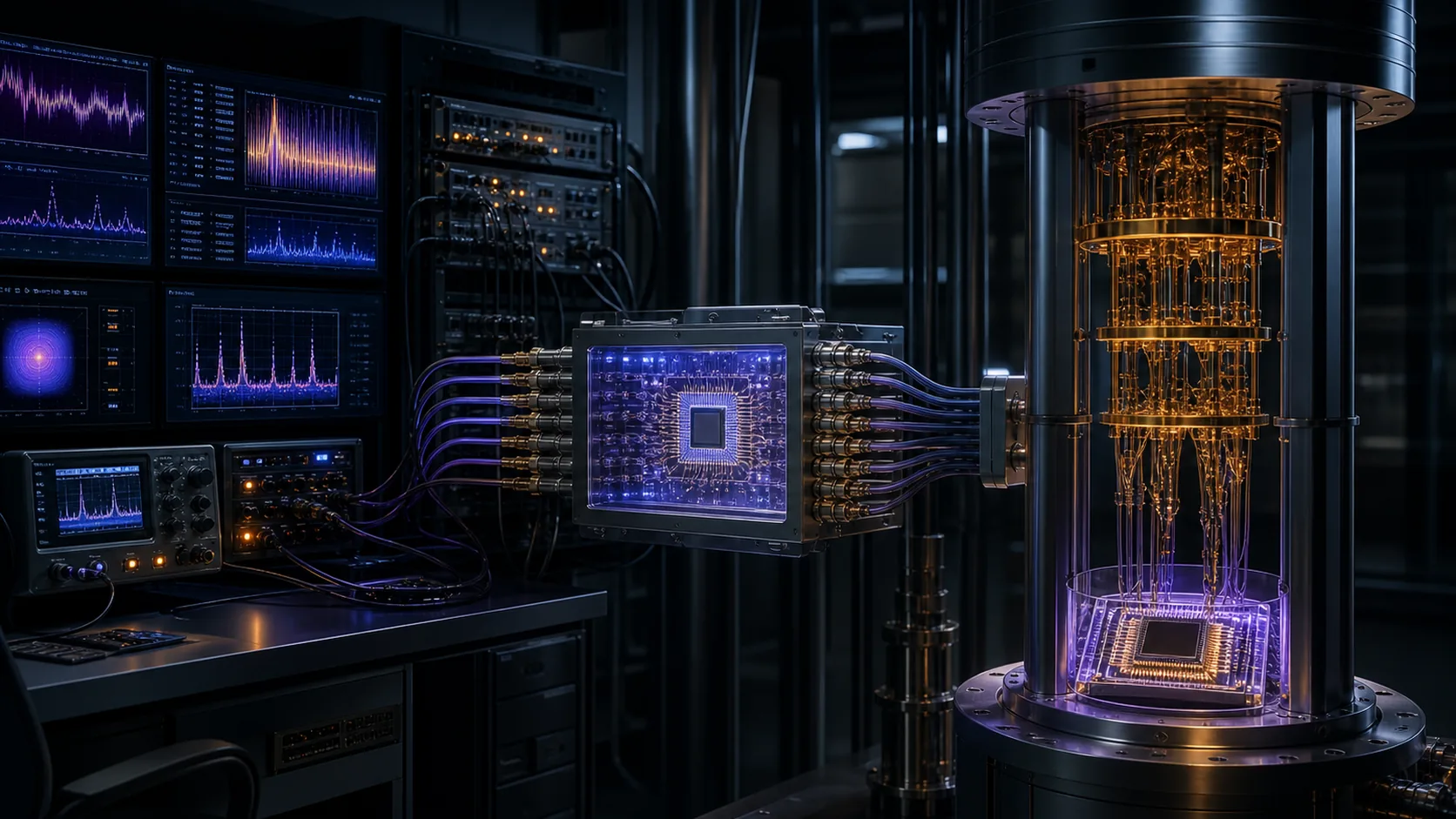
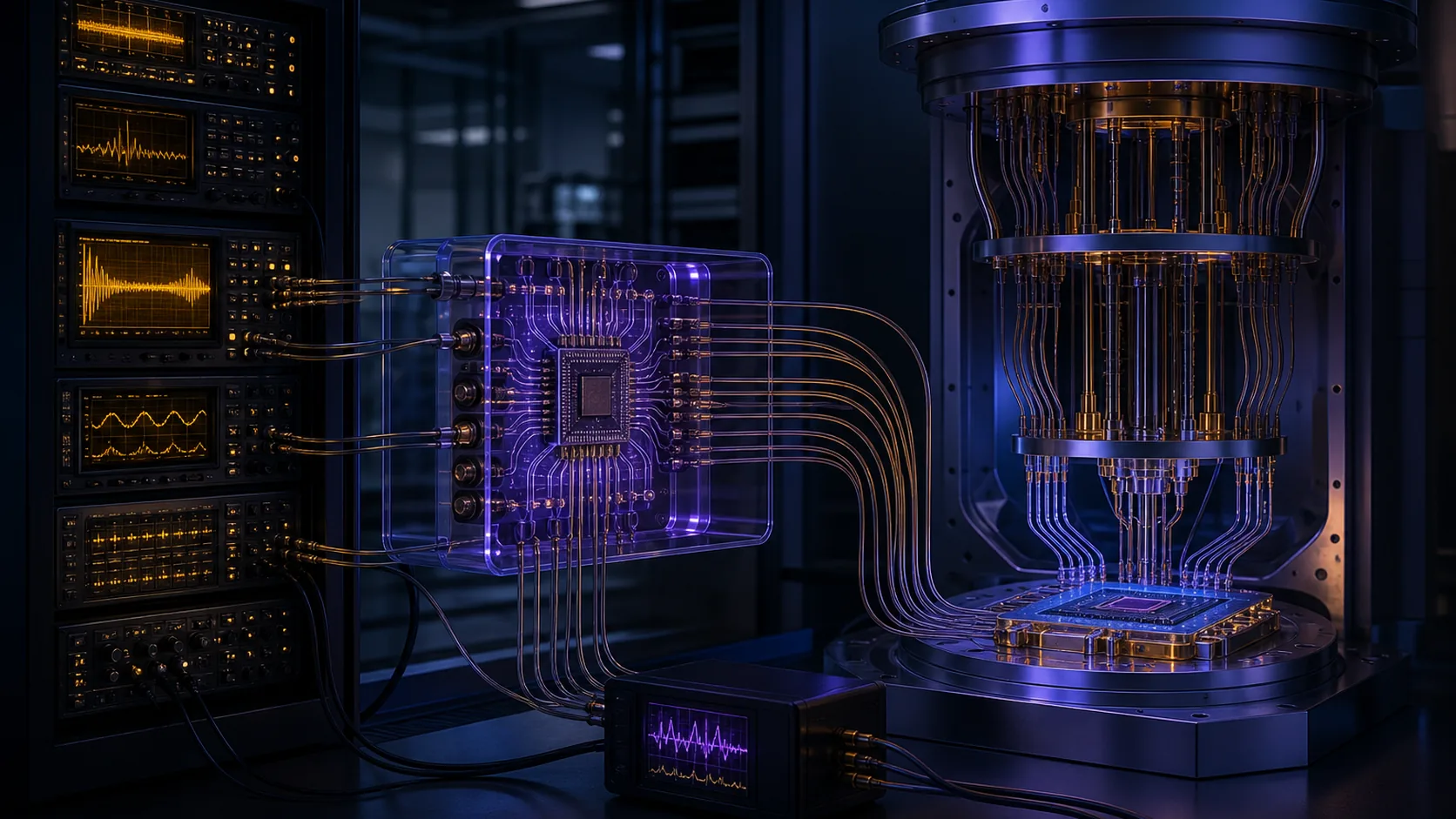
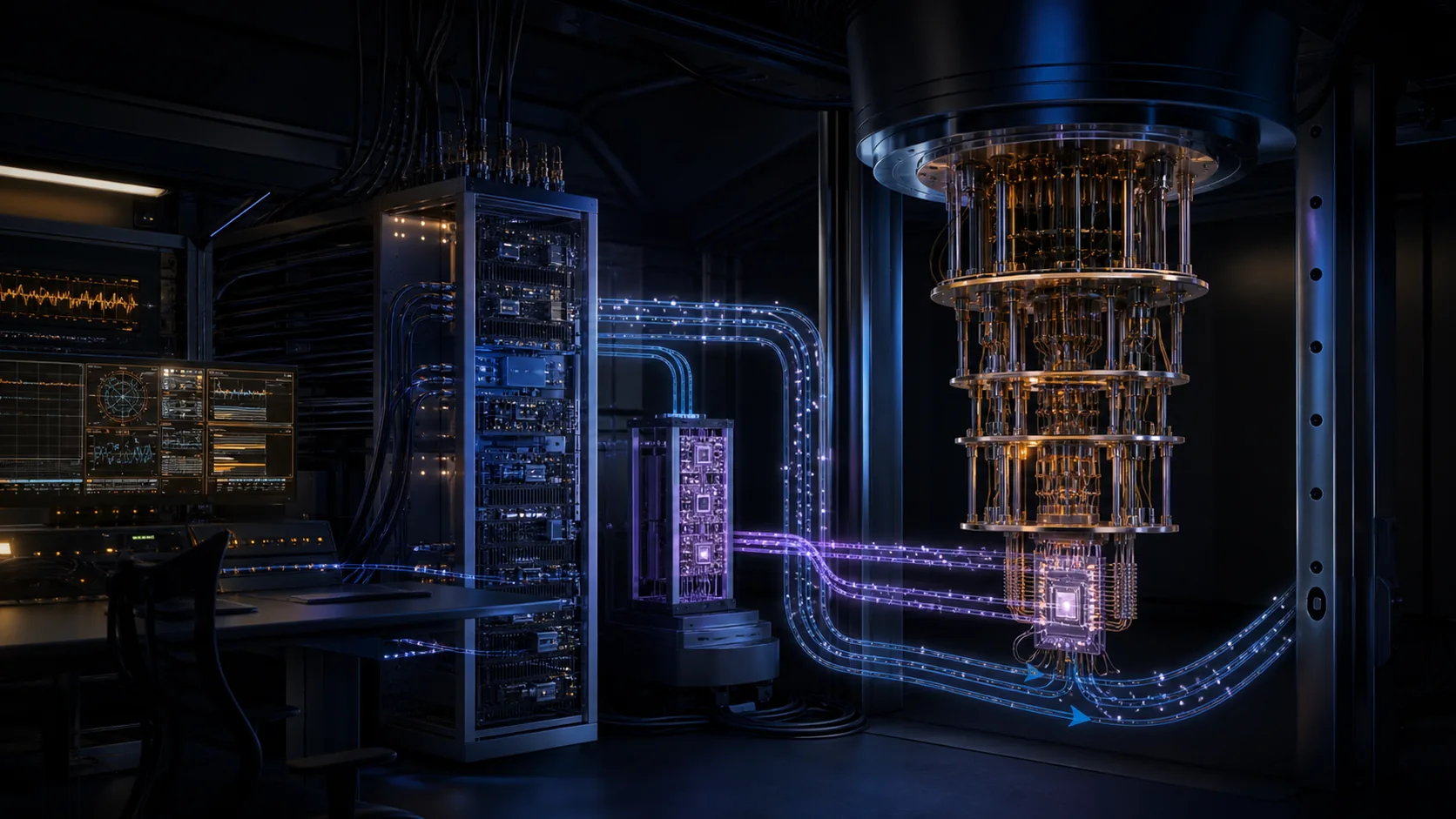
Layer 2, cryo-CMOS control at 4 K (Phase 2, TRL 4 today). Move waveform synthesis inside the cryostat. A control ASIC at the 4 K stage receives a digital instruction stream over a small number of high-bandwidth links and generates many analog drive and flux waveforms locally. What crosses from 300 K is then digital data, not one analog line per qubit. Expected gain: 1.1 paths per qubit down to roughly 0.02. [EST]
The cost is that a control ASIC dissipating even 1 mW per channel over 1.2 million channels is 1.2 kW at 4 K [EST], which is far beyond any 4 K stage. So Layer 2 requires a per-channel power budget of order 10 to 100 uW at 4 K, which is the central device-physics research problem of Phase 2 and should be funded as such from Phase 1.
Layer 3, photonic links (Phase 2 to 3, TRL 3 today). Replace the remaining electrical feedthroughs with optical fibre. Fibre carries far more bandwidth per unit cross-section than coax and conducts substantially less heat. The 2026 literature describes a cryogenic hybrid photonic and CMOS controller architecture aimed at scalable superconducting qubit control. [SRC]
Maturity label, added after cross-review. That source is an architecture-level, first-order feasibility preprint (arXiv:2606.10114v2, June 2026), discussing fan-out groups of 8 to 10 channels replicated to scale, with no stated overall system size target. [SRC] It is not a demonstrated million-channel solution and the earlier draft came close to presenting it as one. Its own scope statement is explicit that the 4 K to millikelvin microwave packaging, which is exactly the interface this plan most needs closed, is left outside its power model. [SRC]
The earlier draft also claimed Layer 3 "eliminates the remaining thermal conduction term." That is too strong and is withdrawn. Optical fibre reduces conducted heat; it does not eliminate the heat load, because the optical-to- electrical conversion at the cold end dissipates power exactly where it is least affordable. Corrected claim: Layer 3 is a candidate architecture for reaching the CRY-1 100 mK allowance, contingent on measured whole-stack heat-load tests that include the conversion stage and the 4 K to millikelvin packaging. [EST]
| Quantity | Value | Basis |
|---|---|---|
| Control channels total | ~2.5 million logical channels | [EST] from A4.3 |
| Waveform update rate | >= 1 GSa/s effective per drive channel | [ASM] for 20 ns gate pulses |
| Readout ADC | >= 1 GSa/s, >= 12 bit | [ASM] standard practice |
| Syndrome data rate, aggregate | 0.66 Tb/s at 1.31M qubits | filled from Codex B1.2, 0.5 bit per physical qubit per 1 us cycle, recomputed at our qubit count |
| Measure-to-feed-forward latency | <= 10 us at p99.9 | [SRC] |
| Room-temperature rack power | 1.5 to 2 MW | [EST] |
The 10 us reaction time is a joint requirement: it spans my readout chain and Codex's decoder. Revised allocation after Codex's B1.2 [EST]: 600 ns measurement acquisition plus reset (his number, not my original 1.0 us), 0.5 us cable and digitizer latency, 0.5 us return path and pulse issue. That leaves 8.4 us for Codex's decoder, slightly more than the 8 us I originally offered.
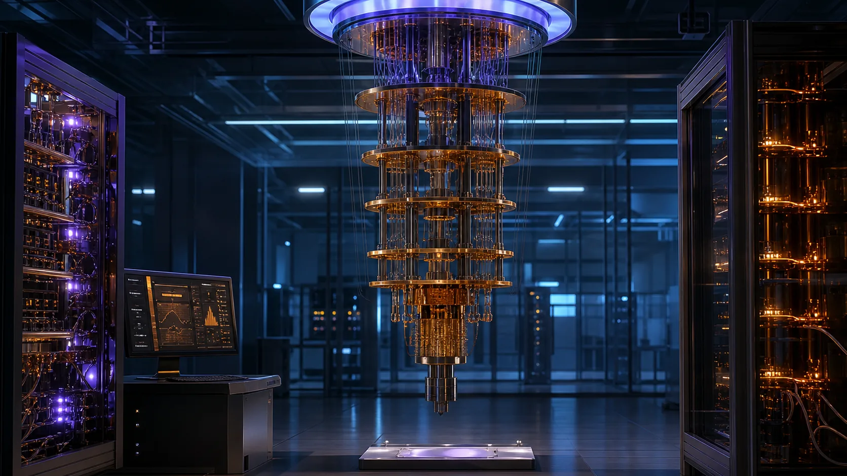
Not "comfortable." The earlier draft called 8.4 us comfortable by comparing it to a reported 124 ns FPGA neural-network decoder latency, a 184 ns throughput period, a 550 ns deterministic closed-loop latency, and a 2.2 us LDPC decode. [SRC] Codex's cross-review rejected that framing and it was wrong: those are small-distance and component-level demonstrations, and mission operation is at distance 25 with surgery traffic, bursts, and simultaneous operation. A sub-microsecond result at distance 3 says very little about distance 25 under load. 8.4 us is an end-to-end acceptance target, not a margin, and it is only demonstrated when measured at mission distance under representative burst and surgery load, per Codex's B3.3 backlog conditions.
Codex's B3.2 correctly points out the harder number I had not confronted: Google reported an average final-decoder latency of 63 us for distance 5 over million-cycle runs [SRC via B3.2]. That is 6x over the whole reaction budget, not just his share. The 10 us target is therefore aggressive against measured practice, and B3.2 is right to call it "aggressive but grounded." It is a real program risk and I have added it to A9 as H13.
On syndrome bandwidth, Codex's instruction to extract detector events next to the readout electronics and ship sparse events rather than raw ADC traces is a hard requirement on my design, not a software preference. At 0.66 Tb/s of raw syndrome, centralized export is not buildable. This is now a constraint on the cryo-CMOS ASIC in A5.2 Layer 2: it must do detector extraction on-die.
Codex's cross-review asked for every thermal stage to be closed with uncertainty ranges, not just 100 mK. The 4 K stage is where cryo-CMOS actually lands, and it is the stage the earlier draft never costed. Doing so now produces the most uncomfortable number in Part A.
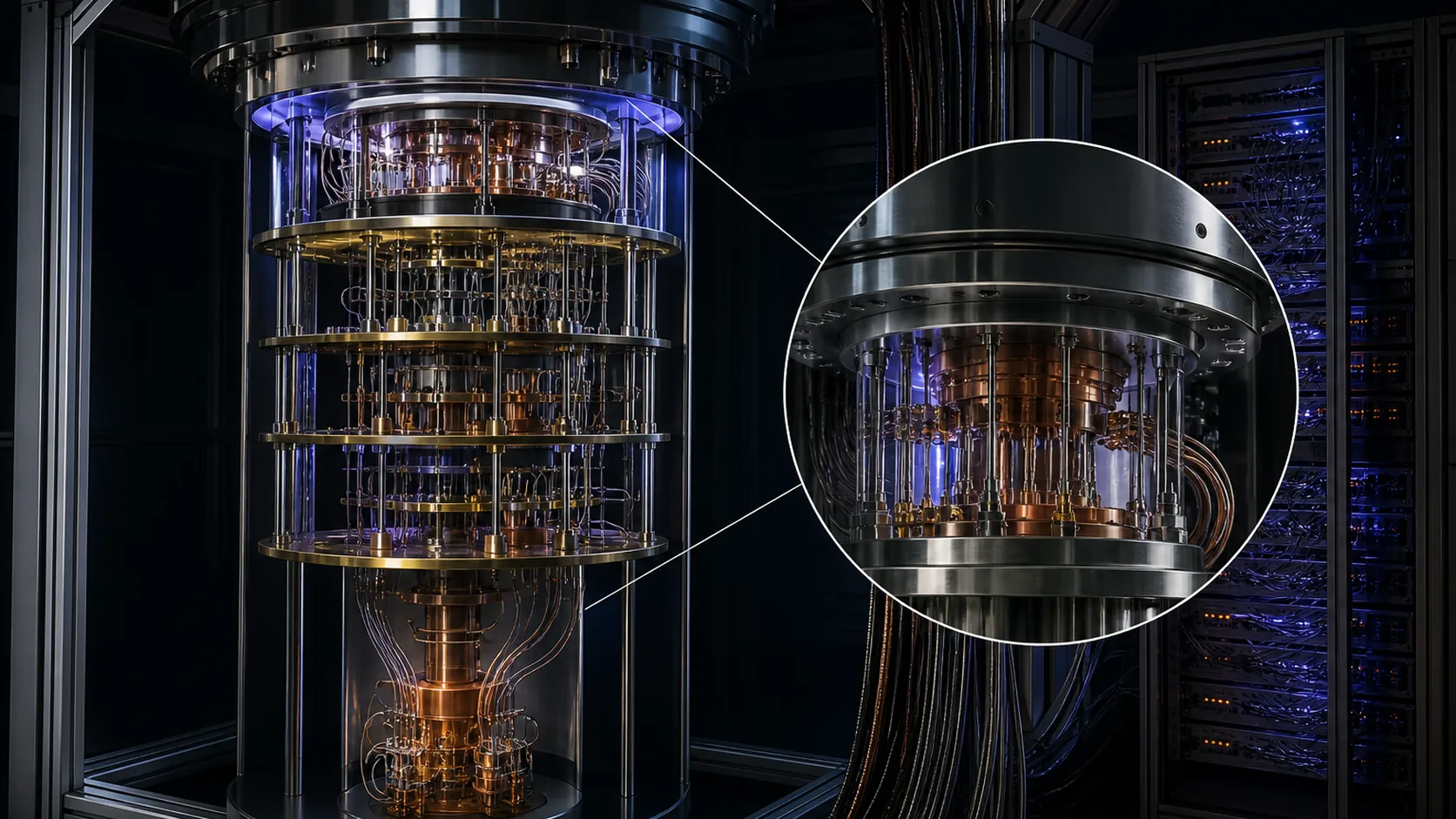
The cited controller architecture gives per-channel dissipation at 4 K of about 48 uW/ch nominal and about 0.66 mW/ch conservative [SRC], against an RF-AWG reference baseline of 0.53 mW/ch nominal and 2.10 mW/ch conservative. [SRC] Applying those to this plan [EST]:
| Case | Per channel at 4 K | 1.2M channels, whole machine | Per cryostat (65,536 ch) |
|---|---|---|---|
| Nominal | 48 uW | 57.6 W | 3.1 W |
| Conservative | 0.66 mW | 792 W | 43.3 W |
| RF-AWG baseline, nominal | 0.53 mW | 636 W | 34.7 W |
| RF-AWG baseline, conservative | 2.10 mW | 2,520 W | 165 W |
For scale, a large dilution refrigerator's 4 K stage is served by pulse tubes delivering on the order of 1.5 to 2 W each at 4.2 K [EST], so a KIDE-class system with three cooling units is in the several-watts class, not the tens or hundreds of watts class.
Reading the table honestly:
at 4 K is roughly a whole 4 K plant devoted to control electronics, which is demanding but is the right order of magnitude to engineer toward.
an order of magnitude beyond a large system's 4 K capacity. If cryo-CMOS lands at 0.66 mW/ch rather than 48 uW/ch, the A3.2 architecture does not close.
this plan cannot simply scale up conventional room-temperature control.
This vindicates the A5.2 Layer 2 requirement of 10 to 100 uW per channel at 4 K, which was written before this source was consulted and turns out to bracket the nominal figure. But it converts that requirement from an engineering preference into a binary architectural dependency: at 48 uW/ch the machine is buildable, at 0.66 mW/ch it is not, and the gap between those two published cases is a factor of 13.75. Closing it is the highest-value research item in the programme.
Two further stages remain incompletely closed and are recorded as gaps:
[SRC] At 65,536 qubits percryostat that is 1.4 nW per qubit [EST]. Nothing in this plan has been costed against that budget.
[SRC] and unaddressed here.
Stated now, in writing, so it is not improvised later. If at the Phase 2 gate we have achieved only Layer 1 and partial Layer 2, say 1 feedthrough per 20 qubits and 0.5 uW per qubit at 100 mK, then Phase 3 needs 200 cryostats rather than 20 [EST], capital cost roughly triples, and the fallback trigger in A2.4 fires. The correct response in that case is to switch the primary modality to neutral atom and accept the slower clock, not to build 200 cryostats. A neutral atom machine has no dilution refrigerator in the qubit path at all, which is precisely why it is the right hedge against a cryogenic wiring failure.
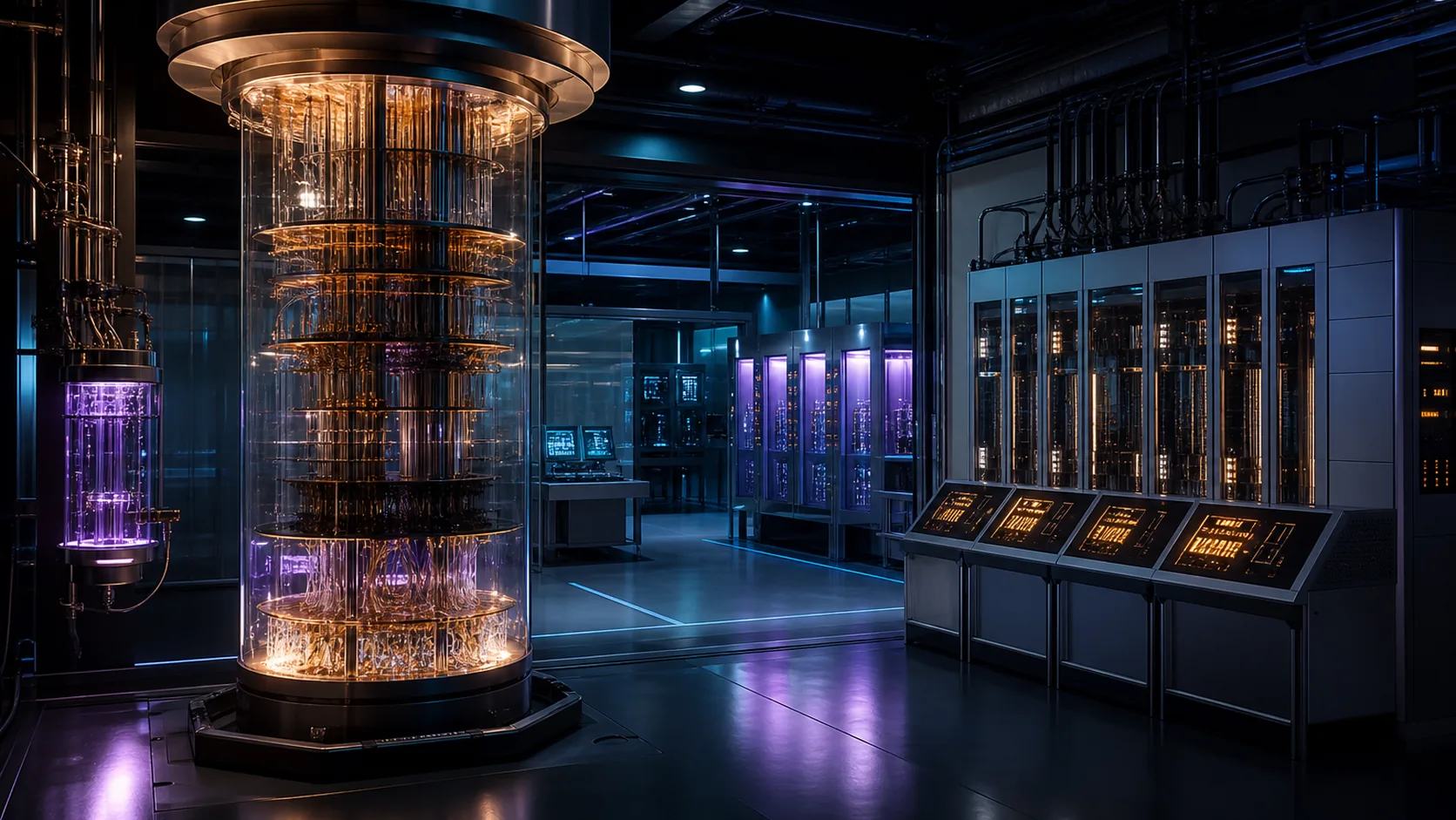
Tantalum base layer on high-resistivity silicon substrate, selected because it delivers millisecond-class lifetimes and coherence with an explicit path to wafer-scale fabrication. [SRC] Losses in this class of device are dominated by two-level systems with comparable contributions from surface and bulk dielectrics [SRC], so the process control priorities are, in order: surface preparation and interface cleanliness, chemical mechanical planarization of the tantalum [SRC], junction barrier uniformity, and packaging-induced loss.
Chosen over the tantalum-on-sapphire variant because sapphire does not ride the silicon CMOS supply chain, and Phase 3 needs 1,200 wafers of yielded parts, not laboratory one-offs.
[SRC]screening as the junction uniformity proxy.
[SRC] IBM Loondemonstrates multi-layer routing on chip.
[SRC] Mechanicallyintermixed indium superconducting connections are demonstrated for microwave quantum interconnects.
[SRC]There is no published wafer-scale yield figure for this device class that we should treat as authoritative, so this is an explicit model [EST], and it is the number most likely to be wrong in Part A.
Let p be the probability that one physical qubit lands within its frequency and coherence acceptance window. A module of 1,024 qubits is usable if a repair-free core plus a spare pool meets spec. With frequency-tunable couplers, individual dead qubits can be masked out of the lattice at a code-distance cost.
| Per-qubit yield p | Expected dead qubits per 1,024 module | Usability |
|---|---|---|
| 0.90 | 102 | Not credible at any layout |
| 0.97 | 31 | Undetermined |
| 0.99 | 10 | Undetermined |
| 0.995 | 5 | Undetermined |
The right-hand column previously asserted that 10 dead qubits per module were "absorbable by defect-aware surface code" and that 5 were "comfortable." Both claims are withdrawn. They were unsupported, and Codex's cross-review is correct that they cannot be recovered from a per-qubit yield figure at all, for the reasons in the next paragraph. Only the top row survives, and only because 102 dead qubits in a 1,024-qubit module is implausible under any layout.
Note also that this table counts qubit yield only. It says nothing about coupler, readout, reset, junction-correlation, crosstalk, or frequency-collision defects, each of which can render a physically working qubit unusable.
Requirement FAB-1. Achieve p >= 0.99 at module scale by the Phase 2 gate. [ASM]
Codex's answer, and why FAB-1 stays an assumption. I asked him for a single defect-tolerance number to size this spec against. He declined to give one, and the refusal is better engineering than a number would have been. His B1.4 states: do not convert a bare fabrication-yield percentage into logical capacity; ingest the measured qubit, coupler, readout, reset, crosstalk, and frequency-collision defect map, then rerun routing and circuit-level logical simulation, because a region is usable only if its deformed patches retain their effective distance. The reserve stays an uncertainty band until measured spatial defect correlations and layout Monte Carlo support a specific allowance.
He is right, and the reason exposes something the table above hides: it treats dead qubits as independent, which is the assumption most likely to be false. Fab defects cluster, and frequency collisions are not independent of layout. A module with 10 scattered dead qubits and a module with 10 dead qubits in one corner have identical p and completely different logical capacity.
FAB-1 therefore remains [ASM] and unvalidated, and the honest statement is that Part A cannot presently justify its own fab spec. Closing it needs the measured defect map and layout Monte Carlo that B1.4 specifies, which is Phase 1 work. Recorded in A11.4.
Oxygen-free copper carrier with PCB and SMA or SMP connectors. [SRC] Nested shielding: innermost superconducting niobium or lead can for high-frequency field rejection, outermost mu-metal can for DC field rejection. [SRC] Eccosorb IR filters at cold plate and mixing chamber with cutoff above 100 GHz. [SRC]
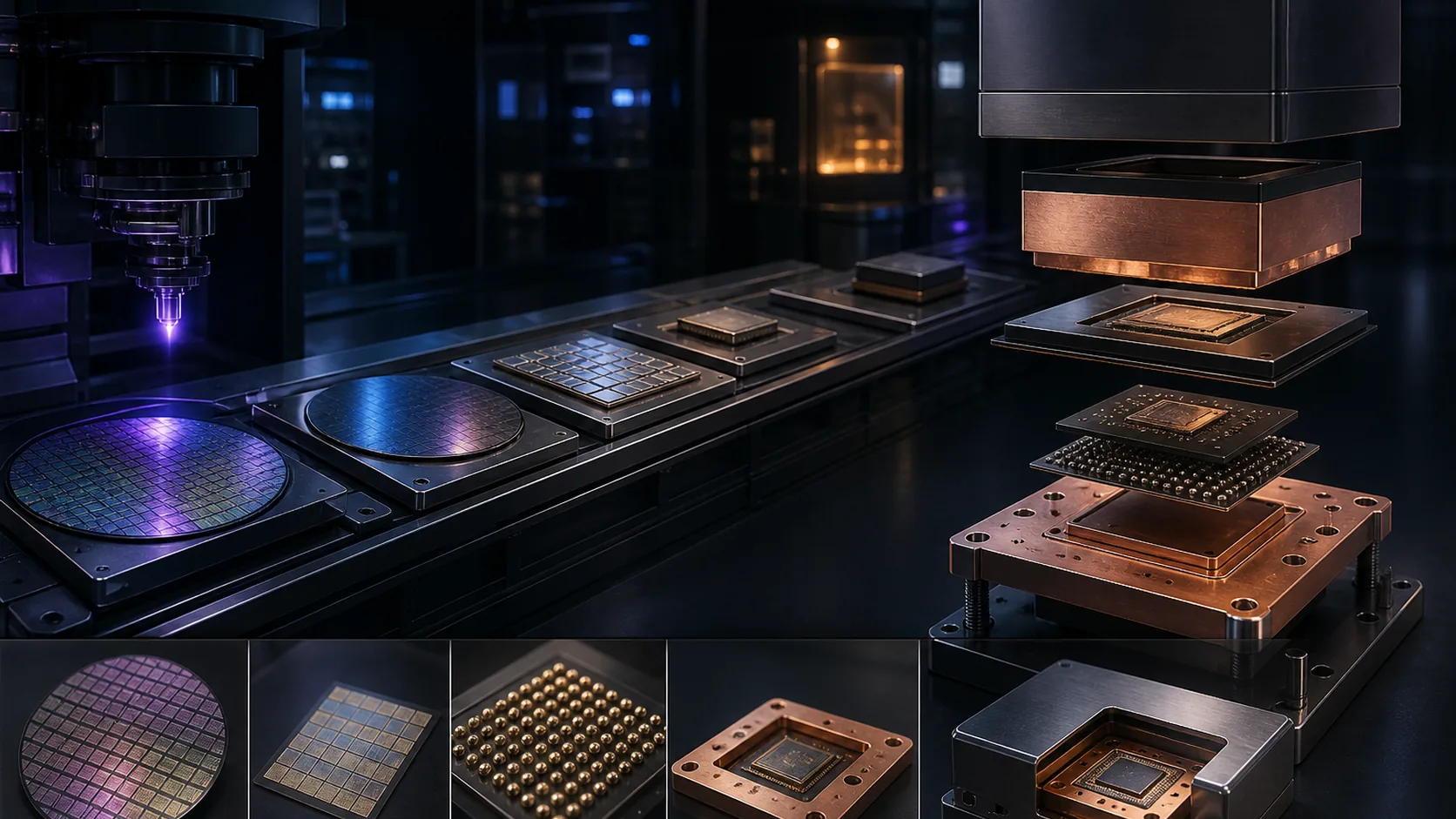
At cluster scale (8 modules) the shielding problem changes character: the cans must enclose a much larger volume while maintaining the same residual field, and crosstalk between modules becomes a first-order design constraint rather than an afterthought. Budget dedicated electromagnetic modelling from Phase 1.
Covered quantitatively in A4.6. Safety items specific to this build:
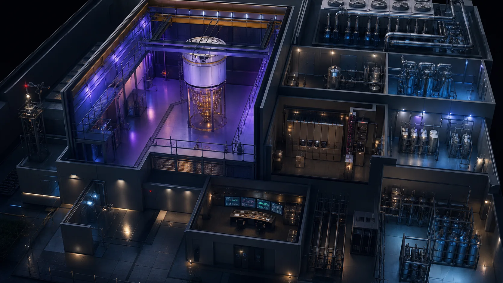
distributed oxygen monitoring with local alarms, forced ventilation interlocked to the monitors, and a written confined-space procedure.
worst-case vacuum-jacket failure.
legal and financial requirement, not good practice. [SRC]
becomes a dominant facility concern instead of the helium hazards.
Uptime and maintenance drivers [SRC]: pulse-tube cold-head service every 18 to 24 months, annual compressor adsorber replacement, annual helium-3 mixture check, gas-handling filter replacement every 12 months, and at least one planned warm-up per year costing 5 to 10 days of downtime. Unplanned recovery runs 5 to 10 days at $10K to $50K per day. [SRC]
At 20 cryostats, staggered maintenance means the Phase 3 machine is never fully available. I originally wrote here that the system should let a cryostat go offline while the logical layout is "recompiled around the missing cluster," and asked Codex to add that to B6.
He added it, and corrected me in the process. His B6.3 now states that losing a module or cryostat during a job is not transparent: the runtime may migrate a live logical state only through a tested fault-tolerant protocol with budgeted link operations, and otherwise must reach a syndrome-safe checkpoint, abort the affected execution segment, and restart from a verified checkpoint. Recompiling around an offline region is valid only before state placement or after such a restart.
That correction matters and my original framing was wrong. A logical qubit is not a process that can be rescheduled onto other hardware mid-flight. Its state lives in a specific patch of physical qubits, and if that patch goes away, the state is gone unless it was moved by an explicit, budgeted, fault-tolerant operation first. "The compiler routes around it" was hand-waving on my part.
The real Part A requirements that follow are therefore harder than what I asked for, and they are hardware requirements, not compiler ones:
equipment. A pulse-tube service window that lands mid-job destroys the job.
place a job only on regions that will stay healthy for its full duration. At a 4.96 day RSA run [SRC], that is a five-day no-touch guarantee on 20 cryostats.
cold-storage patches, not a software feature.
These are unpriced in A8.3 and are a known gap.
All [SRC]:
| Item | Cost |
|---|---|
| QuantWare Soprano-D5, 5 qubits | ~EUR 60K |
| QuantWare Contralto-D21, 21 qubits | ~EUR 300K |
| Rigetti Novera 9-qubit QPU | ~$900K, ~$2.85M as a complete system |
| Bluefors LD450sl | $700K to $1M |
| Bluefors XLD1000sl | $1.5M to $2.5M |
| Bluefors KIDE | $5M to $10M |
| Control electronics cluster (Qblox / QM OPX+ / Zurich QCCS) | $200K to $500K |
| Delft Circuits Cri/oFlex wiring assemblies | $50K to $200K |
| Conventional coax, 5-qubit scale | ~$30K |
| Helium-3 initial charge, 40 L at $2,500/L | ~$100K |
| Helium recovery system | ~$80K |
| Calibration software (Q-CTRL, QuantrolOx) | $50K to $80K initial, $30K to $50K annual |
| HPC GPU integration node | $150K to $300K |
| Facility preparation retrofit | $200K to $400K |
| Systems integration services | $200K to $400K, plus $50K to $100K annual |
| Loaded personnel cost | $150K per FTE per year |
Published reference points [SRC]: entry 5-qubit system year-0 capex about $1.96M; five-year TCO about $5.1M for 5 qubits and about $10.1M for 20 qubits; ten-year TCO $50M to $150M at industrial scale; for every dollar of hardware expect $1.60 of operating cost over five years.
Every gate is a functional criterion, not a build criterion. "The fridge is cold" and "the chip yielded" are not gates. Codex owns the acceptance test design in B7, and I will hold the hardware to whatever he specifies.
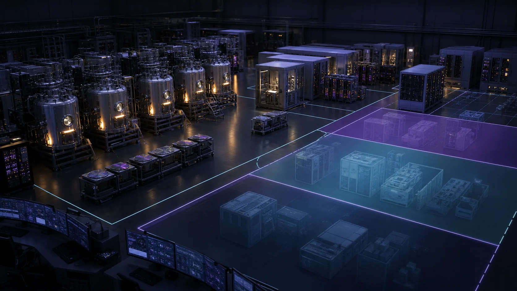
Phase 0. Foundation. Months 0 to 12.
Scope: one XLD1000sl-class cryostat, one 96 to 128 qubit QPU, commodity control electronics, full commissioning discipline. Buy cloud access to a Quantinuum Helios-class trapped-ion machine in parallel so the Part B software stack has a high-fidelity target to develop against from month 1 rather than month 36. [SRC]
Corrected after cross-review. The earlier draft specified a 20 to 30 qubit device and then set a gate requiring a distance-3 to distance-5 surface code memory. Those are incompatible and Codex caught it. A distance-5 rotated patch needs 2d^2 - 1 = 49 physical qubits as raw memory and 2(d+1)^2 = 72 as an active tile [EST], before leakage-removal ancillas, of which the Willow distance-7 experiment used four [SRC]. A 30-qubit device cannot host a distance-5 code at all. The device is resized to 96 to 128 qubits, which also brings it in line with the 105-qubit Willow class that the gate is benchmarked against [SRC], and stays within the 30 to 400 qubit range of an XLD1000sl. [SRC]
Commissioning timeline [SRC]: cryostat install 1 month, wiring tree 1 month, QPU install days, cooldown and readout verification 1 to 2 weeks, single-qubit characterization days to weeks, two-qubit calibration weeks, benchmarking and acceptance 1 to 2 weeks. Total roughly 5 to 8 weeks of commissioning.
Procurement lead time, corrected after cross-review. The earlier draft quoted a generic 3-month site-prep-and-procurement window alongside cryostat lead times of 4 months for an LD450sl and 6 to 12 months for XLD1000sl and KIDE class [SRC], which is internally inconsistent: procurement cannot complete in 3 months when the long-lead item takes 6 to 12. The binding constraint is the cryostat. Phase 0 is therefore planned against a 6 to 12 month cryostat lead, with site prep running inside it, and control-platform FPGA allocation at 8 to 16 weeks [SRC] and TWPA and HEMT spares at multi-month leads [SRC] scheduled inside the same window. Commissioning starts when the cryostat lands, not at month 3.
Gate 0: reproduce a distance-3 surface code memory with real-time decoding, and show error suppression when moving to distance-5. Not "a logical qubit exists," but Lambda > 1 measured on our own hardware.
Cost: $6M capex, $2M opex. [EST] Staff: 6 FTE. [SRC] for the 3 to 5 FTE single-system figure, scaled up for the QEC work.
Phase 1. Logical qubit. Months 12 to 42.
Scope: 1,024-qubit module. One KIDE-class cryostat. Layer 1 multiplexing. In-house tantalum-on-silicon fab line or a firm foundry partnership. Start helium-3 procurement for Phase 3 now (A4.5). Fund the cryo-CMOS per-channel power research (A5.2 Layer 2) as a dedicated workstream from month 12, because it has the longest lead time of anything in the program.
Gate 1, recast as an evidence and scaling gate after cross-review:
distance-7 error per cycle <= 0.143 percent. [SRC]
production module with fitted uncertainty bounds and an explicit test for an error floor, per Codex's B1.4, rather than asserting a single distance.
surgery, with the logical error rate measured, not extrapolated.
The earlier draft asked for a logical error rate <= 1e-6 per logical operation on a 1,024-qubit module. Codex rejected that on two grounds and both are right. First, capacity: two distance-15 active tiles are 2 x 512 = 1,024 physical qubits [EST], exactly the whole module, leaving zero qubits for surgery workspace, routing, or factories, so the configuration the gate implies does not fit. Second, inference: the measured distance-7 result does not imply a distance-15 two-logical-gate error of 1e-6, and Codex's B1.4 explicitly forbids extrapolating mission performance from a single below-threshold distance. The numeric target is therefore withdrawn and replaced by the measurement programme above, which is what actually determines whether Phase 2 is justified.
Cost: $60M capex, $25M opex. [EST] Staff: 45 FTE.
Phase 2. Logical processor. Months 42 to 84.
Scope: 8-module cluster, then multi-cluster. Cryo-CMOS control at 4 K. First photonic link. This is the phase where CRY-1 and FAB-1 are won or lost, and where the A2.4 fallback trigger is evaluated.
Gate 2, corrected after cross-review:
with the 4 K and 20 mK stages closed as well, per A5.4.
by a per-qubit yield percentage.
distributed-overhead multiplier.
production software stack, with the result verified against an independent classical method. Codex specifies these in B7.2: a small factoring workflow on a classically known composite, and a chemistry workflow such as H2 checked against exact diagonalization within the requested tolerance.
The earlier draft made Gate 2 "a chemistry problem that a classical computer cannot do." Codex was right to reject that. A result no classical computer can reproduce is a result nobody can check, which makes it useless as an acceptance criterion: passing it would be indistinguishable from a silent compiler, calibration, or decoder fault producing plausible numbers. The gate that proves the machine works is the one whose answer we already know. Beyond-classical runs are the product; exactly checkable runs are the proof, and they must come first.
Cost: $350M capex, $150M opex. [EST] Staff: 200 FTE.
Phase 3. Utility scale. Months 84 to 144.
Scope: 20 cryostats, 1.31 million physical qubits, roughly 1,500 logical qubits.
Gate 3, as corrected twice below: RSA-2048 factored, executed against a test modulus we generated, under a written disclosure and authorization framework agreed with the sponsor before the run, because a working cryptanalytic capability is a policy artifact and not only a technical one. Plus a chemistry problem sized to the 1.31M machine. No wall-clock target is attached to the RSA criterion at this gate, for the reason in A3.4.
Cost: $2.6B capex, $1.1B opex over the phase. [EST] Staff: 600 FTE.
Scope correction after cross-verification. As originally drafted, Gate 3 claimed both reference workloads. Re-deriving Codex's B5 numbers showed that is false for chemistry, and the arithmetic is in verify/part-b-arithmetic-check.py:
| Workload | Physical qubits required | Phase 3 machine (1,310,720) |
|---|---|---|
| RSA-2048, Gidney 2025 layout | 897,864, recomputed as 1,280 x 430 + 131 x 1,352 + 170,352 | fits, 46 percent margin |
| FeMoco, Lee et al. 2021 full stack | ~4,000,000 | does not fit, short by 2,689,280, needs 3.05x the machine |
| FeMoco, optimistic 1,137-logical variant | 1,537,224 data qubits alone, before factories and routing | does not fit |
First correction, scope. Gate 3 originally claimed both reference workloads. It cannot claim FeMoco: that would have been a promise the hardware cannot keep.
Second correction, runtime. The intermediate revision then read "RSA-2048 in under one week." That is also withdrawn, per A3.4. The under-one-week figure belongs to a monolithic square-lattice machine, and this is 20 linked cryostats. Attaching it to Gate 3 would have reintroduced through the back door exactly the claim A3.4 removed from A1.3.
Gate 3 therefore reads: RSA-2048 factored, plus a chemistry problem sized to the 1.31M machine. A wall-clock criterion is added only once LNK-1 closes and the distributed-overhead multiplier is measured. Until then the honest position is that we can say what the machine will compute but not yet how long it takes.
Phase 4. Chemistry scale. Months 144 to 192. (added after cross-verification)
Scope: expand to 62 cryostats and roughly 4 million physical qubits to reach the Lee et al. FeMoco configuration. Cryogenic plant rises to 0.9 MW, syndrome bandwidth to 2.0 Tb/s [EST].
Gate 4: FeMoco ground state energy to chemical accuracy, checked against an independent method per Codex's B7.2.
Incremental cost: $3.8B capex [EST], excluding the fab line already capitalized in Phase 3. Program capex through Phase 4 becomes $6.8B.
Recommendation: do not commit Phase 4 at program start. Fund it as an option, not a baseline. The reasoning is that the FeMoco requirement is the least stable number in this entire plan. It has moved from ~1e14 T gates (Reiher 2017) to 3.4e8 logical T gates (spectral amplification) [SRC], a factor of roughly 300,000, while the RSA requirement moved 20x in the same period. Spending $3.8B to hedge against an estimate improving that fast is poor capital allocation. Build the modular Phase 3 machine, which is architecturally able to grow, and re-run Codex's resource estimator at the Gate 3 review before committing.
| Line item | Quantity | Unit | Total | Basis |
|---|---|---|---|---|
| Cryostats, KIDE class or successor | 20 | $8M | $160M | [SRC] unit price |
| Helium-3 inventory plus spares | 1,500 L | $2,500/L | $3.8M | [SRC] |
| QPU modules (1,280 at 1,024 qubits) | 1,280 | $150K | $192M | [EST] amortized fab at volume |
| Fab line capitalization | 1 | $400M | $400M | [EST] |
| Cryo-CMOS control ASICs, NRE plus volume | - | - | $350M | [EST] |
| Photonic interconnect | - | - | $180M | [EST] |
| Room-temperature control racks | - | - | $250M | [EST] |
| Decoding compute | - | - | $200M | facility reservation, not a validated estimate; see below |
| Wiring, interposers, packaging | - | - | $220M | [EST] |
| Facility, 6 MW, 5,000 sq m, UPS, chilled water | 1 | $300M | $300M | [EST] |
| Subtotal before contingency | - | - | $2,256M | [EST] |
| Integration, test, spares, contingency at 15 percent | - | - | $338M | [EST] |
| Phase 3 capital total | ~$2.6B | [EST] |
The earlier draft presented a single $4.3B figure. Codex's cross-review was right to reject that: the estimate rests on a 65.5x cryostat extrapolation (A3.3), an unclosed 4 K budget spanning a factor of 13.75 (A5.4), an unvalidated decoder line, and no vendor quote for the fab, ASIC, or facility, which are 40 percent of Phase 3 capital. A point estimate on those foundations is false precision.
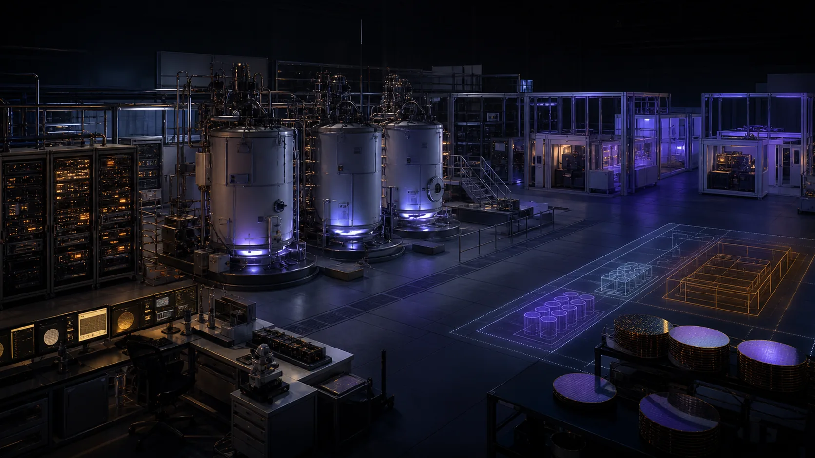
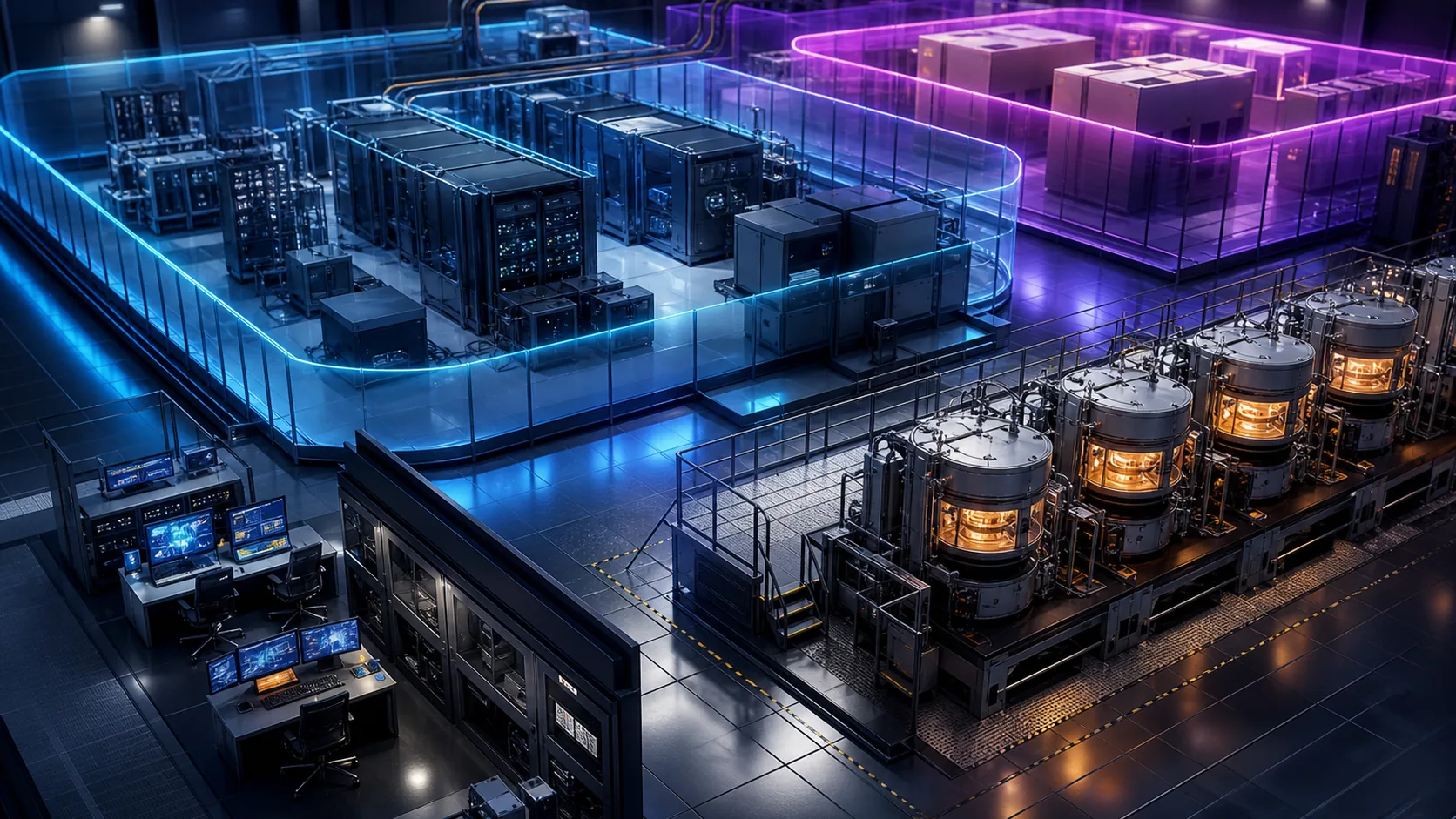
Three cases [EST]. The high case is not a percentage uplift; it is derived from the conservative cryo-CMOS figure in the cited source.
| Low | Base | High | |
|---|---|---|---|
| Driving assumption | CRY-1 overperforms, 14 cryostats, foundry partner shares fab capitalization | as specified in A8.3 | cryo-CMOS lands at 0.66 mW/ch, the source's conservative case [SRC] |
| Cryostats | 14 | 20 | 174 |
| Phase 3 capital | $1.8B | $2.6B | $6.1B |
| Program capital through Phase 3 | $2.2B | $3.0B | $6.5B |
The high case derivation: at 0.66 mW per channel and 65,536 channels per cryostat, the 4 K load is 43.3 W against roughly 5 W of realistic 4 K capacity, a factor of 8.7. Carrying the same total load then needs about 174 cryostats rather than 20 [EST]. The cost of this machine is not primarily driven by qubit count. It is driven by one unresolved number in a cryo-CMOS power budget.
Explicit exclusions from all three cases: Phase 4 (A8.2), decommissioning, helium-3 price escalation, the checkpoint-storage and spare-capacity costs identified in A7, and any distributed-overhead cost arising from A3.4.
Program total across all four phases, base case [EST]: roughly $3.0B capital and $1.3B operating over 12 years, about $4.3B combined, with the range above.
Items in A8.3 and A8.4 that are assumptions, not quotations [ASM], flagged after cross-review: the 1,200-wafer figure in A6.1, the per-wafer and per-module costs, the defect reserve, the 95 percent availability target, all staffing numbers, the entire schedule, and the fab, ASIC, photonic, decoder, and facility lines. The only quoted figures in the cost model are the small-system anchors in A8.1 [SRC], which describe 5 to 20 qubit systems.
The cost shape is the interesting result, and it is not the one most people expect. The QPU modules, the actual qubits, are $192M, which is 7 percent of Phase 3 capital [EST]. The fab line, control ASIC program, and facility are 40 percent; add the photonic interconnect and room-temperature racks and the control and infrastructure block is 57 percent [EST]. Refrigerators are 6 percent.
This inverts the small-scale published ratio, where the cryostat and its support systems are 30 to 50 percent of capital [SRC]. At Phase 3 scale, cryogenics has become a rounding error and the machine is overwhelmingly a control-electronics and semiconductor-manufacturing program that happens to have qubits in it. Any org chart, vendor strategy, or hiring plan that treats this as a physics program with an engineering department attached will fail on cost grounds before it fails on physics.
On the decoding compute line, after Codex's B3.4. I asked Codex to replace my $200M and 1 to 3 MW placeholder. He declined to give a number, and he is right to decline. What he supplied instead is a feasibility anchor: a Collision Clustering decoder ASIC at 0.06 mm^2 and 8 mW covering a surface-code memory of up to 1,057 physical qubits [SRC via B3.4], which linearly projected is about 7.6 W of decoder-core power per million physical qubits. I recomputed this independently: 8 mW x (1e6 / 1057) = 7.57 W, and at our 1,310,720 qubits, 9.9 W [EST].
That number is worth pausing on. The decoder cores for the entire Phase 3 machine draw about ten watts, roughly one millionth of my 1 to 3 MW placeholder. The placeholder is not thereby wrong. It means essentially none of the decoding power is the decoding. It is all detector extraction, I/O, memory, network fabric, hosts, redundancy, the audit decoder, power conversion, and cooling, which is exactly the list B3.4 says its anchor excludes.
The engineering consequence for Part A: the classical side of this machine is a data-movement problem, not a computation problem. That reinforces the A5.3 requirement that detector extraction happen on the cryo-CMOS die. Every syndrome bit that has to travel is far more expensive than the arithmetic performed on it.
Per B3.4, the $200M line is reclassified from an estimate to a facility reservation. It stays in the total so the total is not understated, but it is not a validated figure and must not be presented as one until the B3.4 gate passes: operate a decoder service at no less than one percent of the next phase's syndrome load, measure power at the facility feed, and obtain dated vendor quotes.
| Function | Phase 0 | Phase 1 | Phase 2 | Phase 3 |
|---|---|---|---|---|
| Cryogenics and facility | 1 | 5 | 20 | 60 |
| Fab and materials | 0 | 10 | 45 | 130 |
| Control electronics and RF | 2 | 10 | 45 | 120 |
| QEC, decoding, compiler (Part B) | 1 | 12 | 55 | 170 |
| Applications and verification | 1 | 4 | 20 | 60 |
| Operations, SRE, integration | 1 | 4 | 15 | 60 |
| Total FTE | 6 | 45 | 200 | 600 |
Baseline production role mix [SRC]: 1 facility and cryogenic engineer, 1 to 2 quantum control specialists, 1 HPC/DevOps engineer, 1 to 2 software engineers, and 1 site-reliability rotation, per operating system.
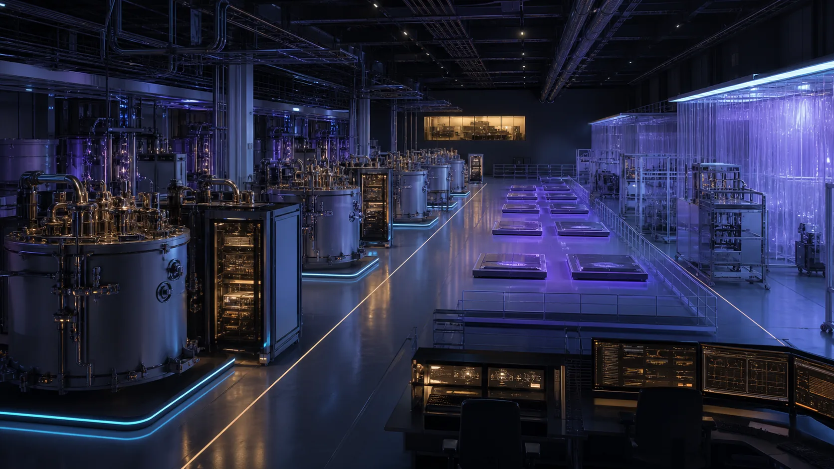
Probability and impact are [ASM] judgments. Exposure is probability times impact on a 1 to 5 scale each.
| ID | Risk | P | I | Exp | Mitigation | Trigger to act |
|---|---|---|---|---|---|---|
| H1 | CRY-1 not met, wiring wall stands | 4 | 5 | 20 | Three independent layers (A5.2), funded in parallel not in series; neutral atom fallback | Phase 2 gate |
| H2 | Cryo-CMOS per-channel power stalls above 100 uW at 4 K | 4 | 4 | 16 | Fund from Phase 1 as its own workstream; second-source two ASIC vendors | Month 30 review |
| H3 | Module yield p stays below 0.99 | 3 | 4 | 12 | Defect-aware code layout (Codex, B2); over-provision qubits per module; in-line junction resistance screening | Phase 1 gate |
| H4 | Helium-3 supply cannot deliver 1,500 L | 3 | 4 | 12 | Begin procurement at Phase 1; closed-loop recovery mandatory; evaluate He-3-free alternatives | Month 18 |
| H5 | Two-qubit fidelity plateaus at 99.5 percent instead of 99.9 | 3 | 5 | 15 | Materials program on TLS loss; if it plateaus, Codex must raise code distance, which raises physical qubit count roughly as d^2 | Phase 1 gate |
| H6 | Inter-module link fidelity too low for logical patches to span modules | 3 | 4 | 12 | A3.1 forces this to be exercised from Phase 2, not discovered at Phase 3; multi-chip tunable coupler and microwave photonic link pursued in parallel | Phase 2 gate |
| H7 | Facility power or siting unavailable at 6 MW | 2 | 4 | 8 | Site selection at Phase 1, co-locate with existing HPC facility | Month 24 |
| H8 | Crosstalk and shielding fail at cluster scale | 3 | 3 | 9 | Dedicated EM modelling from Phase 1; measure at 2-module scale before committing to 8 | Phase 1 gate |
| H9 | Mid-job loss of a module or cryostat destroys the run | 4 | 4 | 16 | Rewritten after cross-review. Loss is not transparently recompilable once a region holds live logical state (Codex B6.3). Mitigations are admission-time placement onto regions guaranteed healthy for the full job duration, declared spare capacity, syndrome-safe checkpoints with physical cold-storage patches, and job-boundary-aligned maintenance. A 4.96 day run needs a five-day no-touch guarantee across 20 cryostats. All three are unpriced in A8.3 | Phase 2 |
| H10 | Single-vendor dependency on Bluefors-class cryostats | 3 | 3 | 9 | Qualify Maybell as second source from Phase 1 [SRC] | Month 18 |
| H11 | A working RSA-2048 capability creates disclosure and policy obligations | 5 | 3 | 15 | Written authorization and disclosure framework agreed before Gate 3; run only against self-generated test moduli; coordinate with post-quantum migration stakeholders | Phase 2 |
| H12 | Published resource estimates improve again and the machine is oversized | 3 | 1 | 3 | Not a real risk. Estimates have improved 20x once already [SRC]; a smaller requirement is a schedule gift, and the modular architecture ships value at each phase gate | n/a |
| H13 | 10 us reaction budget unreachable in practice | 4 | 5 | 20 | Added after cross-verification. Codex B3.2 cites a measured 63 us average final-decoder latency at distance 5 [SRC], 6x over the whole budget. Mitigations: detector extraction on the cryo-CMOS die (A5.3), sharded local decoding, ASIC path, and Codex's <= 50 percent utilization rule. If p99.9 misses 10 us, non-Clifford work is blocked and the RSA runtime claim fails | Phase 1 gate |
| H14 | Phase 3 machine cannot reach FeMoco (3.05x short) | 5 | 2 | 10 | Known and accepted, not a surprise. Gate 3 rescoped in A8.2; Phase 4 defined and priced but deliberately not baselined | resolved by scope change |
| H15 | Distributed topology invalidates the RSA runtime | 5 | 4 | 20 | Added after cross-review. The source estimate assumes one square nearest-neighbor grid [SRC]; this is a 20-cryostat machine. A distributed-overhead multiplier of only 1.41 consumes the entire margin to 7 days. Mitigation: LNK-1 acceptance gate in A3.4, and re-run Codex's estimator against the real connectivity graph. Until then the runtime claim is withdrawn, not merely at risk | Phase 2 gate |
| H16 | Cryo-CMOS lands at the conservative 0.66 mW/ch rather than 48 uW/ch | 3 | 5 | 15 | Added after cross-review. The two published cases differ by 13.75x and straddle buildability: 3.1 W per cryostat at 4 K is engineerable, 43.3 W is not (A5.4). The high cost case at $6.1B is this risk landing. Mitigation: fund the per-channel power problem from Phase 1 as the single highest-value research item; qualify two ASIC vendors | Month 30 review |
| H17 | The 20 mK stage is uncosted | 4 | 3 | 12 | Added after cross-review. KIDE gives > 90 uW at 20 mK [SRC], about 1.4 nW per qubit at 65,536 qubits per cryostat [EST]. No element of this plan has been budgeted against it | Phase 1 |
Highest exposure is now a three-way tie at 20 between H1 (the wiring wall), H13 (the reaction time budget), and H15 (distributed topology).
The shape of that result is worth stating plainly. The original draft of this register had none of H13, H15, H16, or H17 in it, and rated H9 at exposure 8 instead of 16. Four of the five highest-exposure risks in this plan were invisible to its own author and were found by an adversarial reader. They were not found by the arithmetic checker either, which passed 73 of 73 while the document contained an unsupported runtime claim, an uncosted cryogenic stage, and a phase gate whose device was too small to run it. Arithmetic verification and assumption verification are different activities, and only the second one found these.
If H1 lands, A2.4 fires and we build a different machine rather than a more expensive version of this one. If H13 or H15 lands, the modality choice in A2.3 is weakened at its foundation, because A1.2's clock-speed argument assumes both that the control loop closes at 1 us and that the distributed machine inherits a monolithic machine's runtime. H13, H15, and A1.2 should be reviewed together at the Phase 1 gate. If H16 lands, the machine costs $6.1B instead of $2.6B.
| # | Question | Status after reading Part B |
|---|---|---|
| 1 | B1 interface numbers | Answered. B1.2 supplied a full interface table. Four of my A1.3 rows were wrong and are corrected. |
| 2 | A5.3 latency split, 8 us offered | Answered and improved. B1.2's 600 ns measure-plus-reset frees 8.4 us. B3.2 also supplied the 63 us measured counter-evidence that became H13. |
| 3 | A6.3 defect tolerance per patch | Answered by refusal, correctly. B1.4 declines to give a single number and requires a measured defect map plus layout Monte Carlo instead, because clustered defects and frequency collisions break the independence my yield table assumes. FAB-1 stays [ASM] and unvalidated. See A6.3. |
| 4 | A8.3 decoding compute cost and power | Answered by refusal, correctly. B3.4 supplies a feasibility anchor (7.6 W of decoder cores per million qubits, which I recomputed as 7.57 W) and an explicit gate, but declines to issue a capital or installed-power figure until that gate passes. My $200M line is reclassified as a facility reservation. See A8.3. |
| 5 | A7 graceful degradation on cluster loss | Answered, and my framing was corrected. B6.3 establishes that losing a module mid-job is not transparent and that recompiling around an offline region is valid only before state placement or after a restart. This makes the requirement harder than I asked for, and it lands on hardware, not the compiler. See A7. |
| 6 | Challenge A1.2, the clock-speed argument | Taken up, and it landed. The challenge did not arrive as a counter-calculation but as a demolition of the comparison itself: the 676x figure was not a valid like-for-like advantage, and clock-speed-only scaling ignores routing, factories, gates, and reliability on both sides. Codex also identified the topology gap now in A3.4, which attacks A1.2 from the other direction. See A2.3, A3.4. |
Items 3 and 4 came back as reasoned refusals rather than numbers, and in both cases the refusal is the better answer: it converted two figures this document had invented into two explicitly bounded unknowns with a defined way to close them. That is a net improvement in honesty even though it removed two numbers.
Item 6 produced the most consequential result. The request was for a counter- estimate showing whether a slower, lower-overhead machine wins on total cost to solution. What came back instead was the finding that neither side of that comparison is currently computable, because the 676x figure was not a valid advantage and the distributed-topology overhead on the superconducting side has never been modelled. The modality decision therefore rests on less quantitative ground than the 385-to-380 score implied, and A2.3 has been rewritten to say so.
Codex's independent review of Part A raised eleven required corrections. All were independently confirmed before being accepted, including refetching the Bluefors KIDE specification and the cryo-CMOS preprint from their primary sources.
| # | Correction | Where it landed |
|---|---|---|
| 1 | Mission sizing: 1.31M cannot support the ~4M FeMoco plan | already actioned; A8.2, J2 |
| 2 | Adopt Part B's logical contract and interface | already actioned; A1.3, A5.3 |
| 3 | Multi-cryostat topology does not inherit the RSA runtime | new A3.4, LNK-1, risk H15; A1.3 runtime withdrawn |
| 4 | 1,024-qubit module is smaller than a d25 tile | A3.1 rewritten, module size now a gated variable with a seam-equivalence requirement |
| 5 | Phase gates not supported by their own device sizes | A8.2 Phase 0 resized to 96 to 128 qubits; Gates 1 and 2 recast |
| 6 | Cryogenic closure against vendor figures, all stages | A3.3 rewritten against the KIDE datasheet; new A5.4 closing the 4 K and 20 mK stages |
| 7 | Evidence maturity and cost ranges | new A8.4 with low, base, high; assumption labels; A5.2 Layer 3 maturity-labelled |
| 8 | Yield cannot be reduced to a per-qubit percentage | A6.3 usability claims withdrawn |
| 9 | Failure recovery is not transparent recompilation | A7 rewritten, H9 rewritten and re-scored |
| 10 | The 676x neutral-atom comparison is invalid | A2.3 rewritten, claim withdrawn |
| 11 | Decoder margin, source traceability, procurement inconsistency | A5.3 "comfortable" withdrawn; A8.2 procurement lead corrected to 6 to 12 months; A12 restructured |
One correction in that list was accepted with a caveat rather than in full: on item 6, the KIDE 20 mK figure of > 90 uW [SRC] was not in Codex's review and was found while verifying it. It produces a tighter constraint than the 100 mK budget the plan had been working to, and it is now risk H17.
This section exists so that a reader can check our claims instead of trusting our summaries. Both scripts are in verify/ and both are runnable.
verify/part-a-arithmetic-check.py, 58 assertions, 0 failures at time of writing. Output saved to part-a-arithmetic-check.output.txt.
The first run failed 4 of 58, all in the A8.3 cost table: contingency was stated as $144M when 15 percent of the subtotal is $338M, the Phase 3 total was stated as $2.4B against a computed $2.6B, program capex was stated as $4.1B against a computed $3.0B, and a claimed "60 percent" cost share was actually 40 percent. All four are corrected in the current text. Correcting the share error is what surfaced the genuinely interesting finding now in A8.3: the QPU modules are only 7 percent of Phase 3 capital.
verify/part-b-arithmetic-check.py re-derives every numeric claim in Part B from its cited inputs rather than reusing Codex's stated results. Output saved to part-b-arithmetic-check.output.txt.
Reproduced independently and confirmed: all ten 2d^2-1 and 2(d+1)^2 values in B1.4; the 0.5 Tb/s syndrome aggregate; the 0.0065 union bound; the 28p^2 suppression to 2.8e-13; the six-factory bank at one CCZ per 25 us and 40,000 CCZ/s; the full RSA layout reconstruction 1,280 x 430 + 131 x 1,352 + 170,352 = 897,864; both Toffoli demand rates (15,168/s and 15,336/s); both 8T-to-CCZ candidate counts; the FeMoco footprint 2,142 x 1,352 = 2,895,984; and the rule-of-three bound requiring 3e15 trials, which I extend to note that at 1 us per trial this is 95 years of continuous running.
One arithmetic error found in Part B, and fixed by its author. B2.1's surface-code weighted total was stated as 440 of 500. Recomputing from Codex's own weights and scores gives 25x5 + 20x5 + 20x2 + 15x4 + 10x5 + 10x4 = 415. The bivariate bicycle total of 260 was correct. The decision was never in doubt: 415 against 260 still selects the surface code as the production baseline, and by a wider relative margin than my own 385-against-380 modality call. I did not edit his file. I sent the correction over the handoff channel and Codex corrected it himself, along with substantive additions to B1.4, B3.4, and B6.3 answering three further gaps I had raised. Part B now reads 415.
Worth recording, because it is the argument for doing it at all. Reading Codex's summary would have caught none of these:
numbers in the same script.
machine 3.05x too small.
converted into explicitly bounded unknowns with defined closure gates, because Codex declined to supply figures that do not yet exist.
mid-job. Correcting it produced three new hardware requirements that neither part had captured.
Then the reverse pass, Codex's independent review of Part A, found eleven more (A10.1), including:
20-cryostat machine, using an estimate whose source assumes a single square nearest-neighbor grid. A distributed-overhead multiplier of 1.41 erases the entire margin, and nobody has measured it.
qubits and then required a distance-5 code needing at least 49.
lands, was never closed. Closing it revealed that the two published per-channel figures straddle buildability by a factor of 13.75.
which divided two incommensurable quantities.
seen.
The arithmetic checker passed 73 of 73 throughout all of that. It could not have caught any of it, because every one of those defects was a sound calculation resting on an unexamined assumption. Checking the arithmetic and checking the premises are different jobs. This document needed both, and needed a second author to do the second one.
Stated plainly rather than implied by omission.
[SRC] figure issomeone else's measurement, and every [EST] is arithmetic on top of those.
real vendor quotes for 5 to 20 qubit systems [SRC]. Extrapolating them to 1.31 million qubits is an assumption, and the fab, ASIC, and facility lines, which are 40 percent of Phase 3 capital, have no vendor anchor at all.
improvement is asserted as a requirement, not shown to be achievable.
No published wafer-scale yield figure for this device class was found, and Codex's B1.4 correctly points out that clustered defects and frequency collisions make a single per-qubit yield number insufficient regardless. FAB-1 cannot be justified until Phase 1 produces a measured defect map.
B3.4's gate has not been passed. The $200M sits in the $2.6B total so the total is not understated, but it is not validated.
Identified only after Codex corrected my graceful-degradation framing in A7.
against an estimate for a machine we are not building. Bounded below by 4.96 days, upper bound unmodelled.
differ by 13.75x and straddle buildability.
is currently justified.
suggests** (A2.3). The comparison that would settle it, same workload and same logical reliability compared on spacetime volume and energy, has not been done by either author.
unresolved cryo-CMOS number, not by qubit count.
Source class matters, and the earlier draft did not distinguish it. Codex's cross-review is right that a secondary aggregator page cannot support a technical claim. Sources below are split accordingly.
Class 1, primary technical. Peer-reviewed papers, preprints, and vendor datasheets. These may support technical claims.
Class 2, secondary commercial. Industry aggregator and cost-guide pages. These may support rough-order-of-magnitude cost anchors only, and every figure in A8.1 drawn from them is a ROM estimate for 5 to 20 qubit systems, not a validated price at this plan's scale. No technical requirement in Part A rests on a Class 2 source.
This part turns the physical machine into a fault-tolerant computing service. It deliberately separates three kinds of number:
The production baseline is a rotated surface-code architecture on a local two-dimensional qubit lattice. Bivariate bicycle quantum low-density parity-check (qLDPC) codes remain a gated research branch because their memory density is compelling, but their connectivity, logical gates, and real-time decoding must be proven on the selected hardware before they can displace the baseline.
Do not design against a single average gate fidelity. The engineering noise model shall contain all of the following and shall be refit from hardware data after every material process, packaging, wiring, or pulse-stack change:
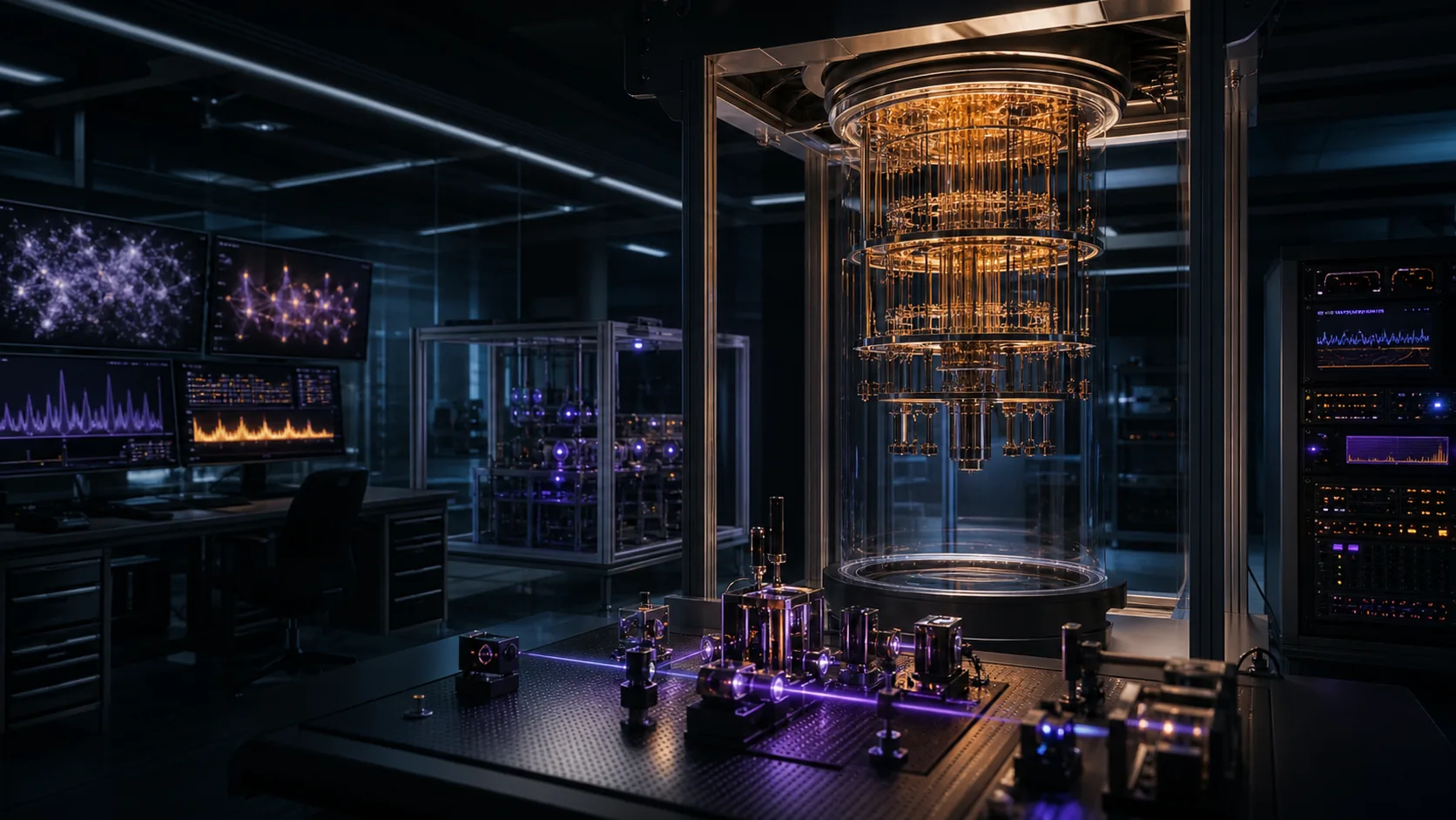
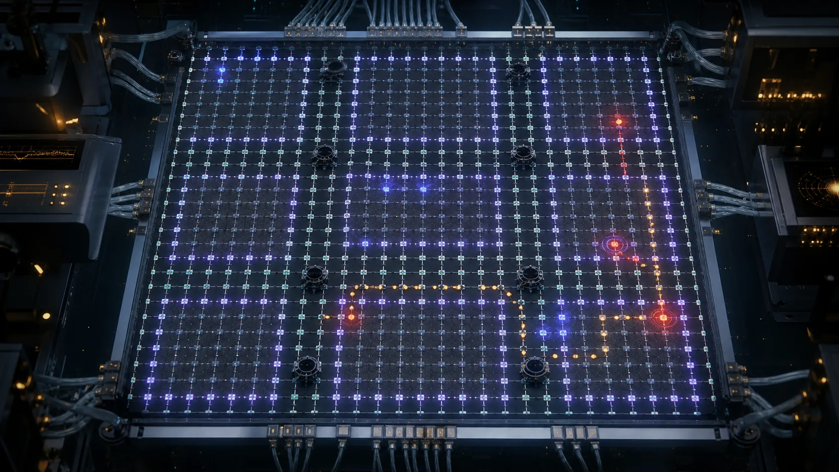
This breadth is mandatory. Google Quantum AI measured a distance-7 surface-code memory at 1.43e-3 logical error per cycle and found that correlated errors contributed an estimated 17 percent of its error budget; its long repetition-code runs also exposed a logical error floor near 1e-10 from rare bursts. Those observations show why an independent and identically distributed depolarizing model is useful for sizing but insufficient for acceptance (Acharya et al., 2024).
| Quantity | Program requirement | Basis and status |
|---|---|---|
| Median one-qubit error per operation | <= 1e-4 | Engineering target. Leaves margin below the uniform 1e-3 circuit-noise assumption used in published large-scale resource estimates. |
| 95th-percentile two-qubit error per operation | <= 1e-3; stretch goal 5e-4 | Engineering target. The primary resource estimates in B5 assume uniform circuit-level error 1e-3. |
| Measurement plus reset error | <= 1e-3 per measured ancilla | Engineering target aligned to the same circuit-level assumption. Report assignment, reset, leakage, and correlated components separately. |
| Measurement acquisition plus reset time | <= 600 ns | Engineering target, leaving time for entangling and single-qubit layers inside a 1 us cycle. Part A must close the actual pulse schedule. |
| QEC syndrome cycle | <= 1 us target; 1.1 us acceptable for the first below-threshold gate | Published resource estimates use 1 us; a recent below-threshold experiment used 1.1 us (Acharya et al., 2024). |
| Classical reaction time | <= 10 us at p99.9 for a feed-forward decision | Engineering target matching the assumption used by the RSA resource estimate in B5. Throughput must also prevent backlog. |
| Logical memory error | <= 1e-15 per hot logical-qubit round for mission-scale runs | Engineering target. This is the value used for hot patches in the RSA estimate, not a present-hardware claim (Gidney, 2025). |
| Non-Clifford resource error | <= 1e-12 per consumed CCZ or Toffoli resource | Engineering target. At 6.5e9 Toffolis this contributes at most 0.0065 expected faults by the union bound. |
| Control addressability | 2 independently scheduled actuation degrees per tunable qubit, plus 1 measurement result per syndrome ancilla | Engineering planning envelope. This describes logical addressability, not a one-cable-per-signal implementation. Part A may multiplex physical lines. |
| Syndrome output | approximately 0.5 raw syndrome bit per physical qubit per cycle | Derived from roughly one measured ancilla per data qubit. At one million physical qubits and 1 us cycles, the unframed aggregate is about 0.5 Tb/s; process and decode locally instead of exporting it centrally. |
For a compiled job, compute an error ledger by operation class. In the low-error regime, the conservative first check is the union bound
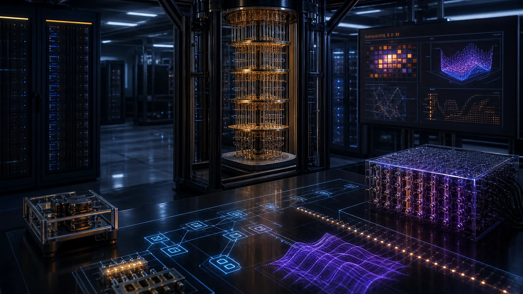
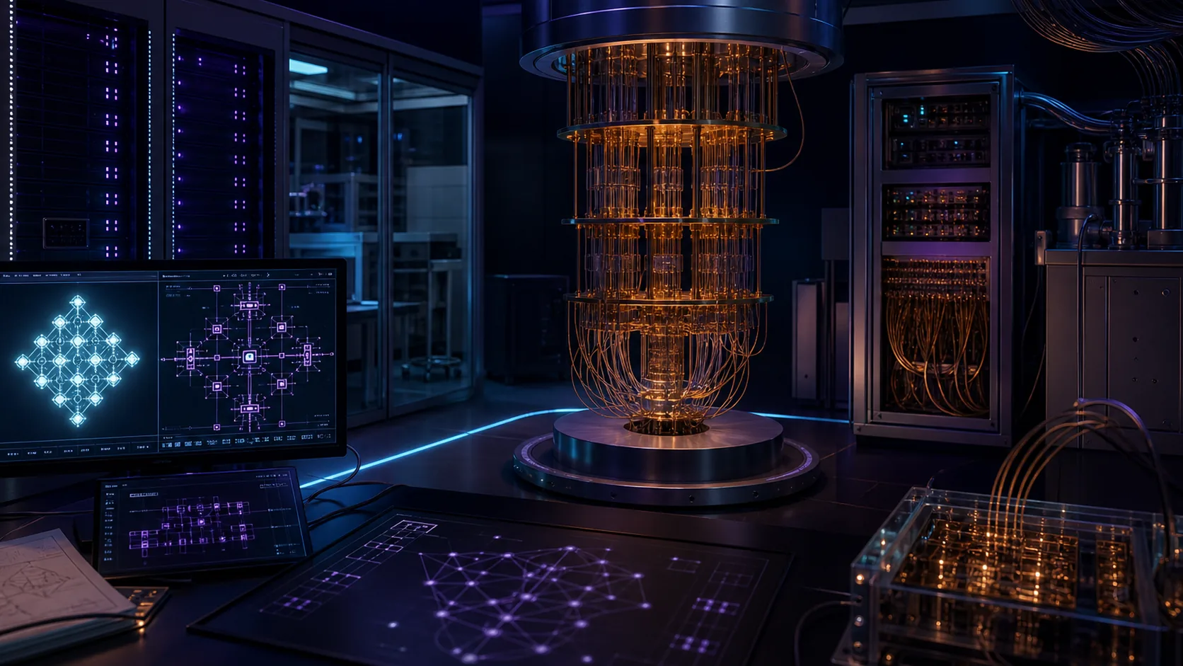
P_fail <= sum_i(N_i * p_i)
where N_i is the number of opportunities for failure of class i and p_i is its validated logical failure probability. Correlated mechanisms require a joint model and may not be multiplied as if independent.
Use this planning allocation for a mission job with required success probability of at least 90 percent. These percentages are engineering allocations, not measurements:
| Failure class | Share of 10 percent job budget |
|---|---|
| Logical memory and Clifford operations | 35 percent |
| Non-Clifford state production and consumption | 20 percent |
| Logical measurement and feed-forward | 15 percent |
| Correlated and burst errors | 15 percent |
| Compiler, scheduler, decoder, and runtime faults | 5 percent |
| Unallocated reserve | 10 percent |
No phase may consume the reserve by changing a spreadsheet alone. A changed allocation requires new circuit counts, measured error distributions, and a reviewed failure-budget calculation.
Select code distance from measured logical scaling, not from a threshold slogan. The raw rotated planar memory uses approximately 2d^2 - 1 data and measurement qubits. For active lattice-surgery planning, use the more conservative 2(d + 1)^2 physical qubits per logical tile, as used in the RSA study. Neither expression includes all routing, factory, spare, or defective-device reserve.
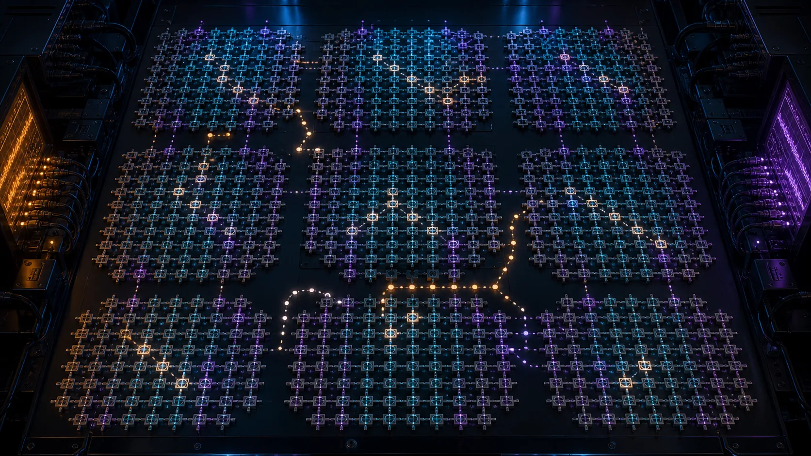
Do not convert a bare fabrication-yield percentage into logical capacity. Before placement, ingest the measured qubit, coupler, readout, reset, crosstalk, and frequency-collision defect map and rerun routing plus circuit-level logical simulations. A region is usable only if its deformed patches retain their effective distance and pass the logical-scaling gate. The physical-qubit reserve remains an uncertainty band until measured spatial defect correlations and layout Monte Carlo results support a specific allowance.
Distance d | Raw memory patch, 2d^2 - 1 | Active tile, 2(d + 1)^2 | Intended program use |
|---|---|---|---|
| 7 | 97 | 128 | Below-threshold memory demonstration |
| 11 | 241 | 288 | Early logical Clifford and lattice-surgery work |
| 15 | 449 | 512 | Pilot fault-tolerant workloads |
| 21 | 881 | 968 | Intermediate mission rehearsal |
| 25 | 1,249 | 1,352 | Initial mission-scale sizing assumption |
The distance-7 Google experiment used 101 qubits after four leakage-removal qubits were added, which is consistent with the raw 97-qubit patch plus mitigation hardware (Acharya et al., 2024). Its measured suppression factor was only Lambda = 2.14 +/- 0.02 for each distance increase of two. Therefore, this program shall not claim 1e-15 logical performance by extrapolating the present distance-7 result. Before mission sizing is frozen, demonstrate below-threshold behavior at three or more distances on the production module, fit uncertainty bounds, test for an error floor, and repeat under simultaneous operations and long-duration drift.
Scores are program judgments on a 1 to 5 scale, where 5 is best. They must be revisited at every architecture gate.
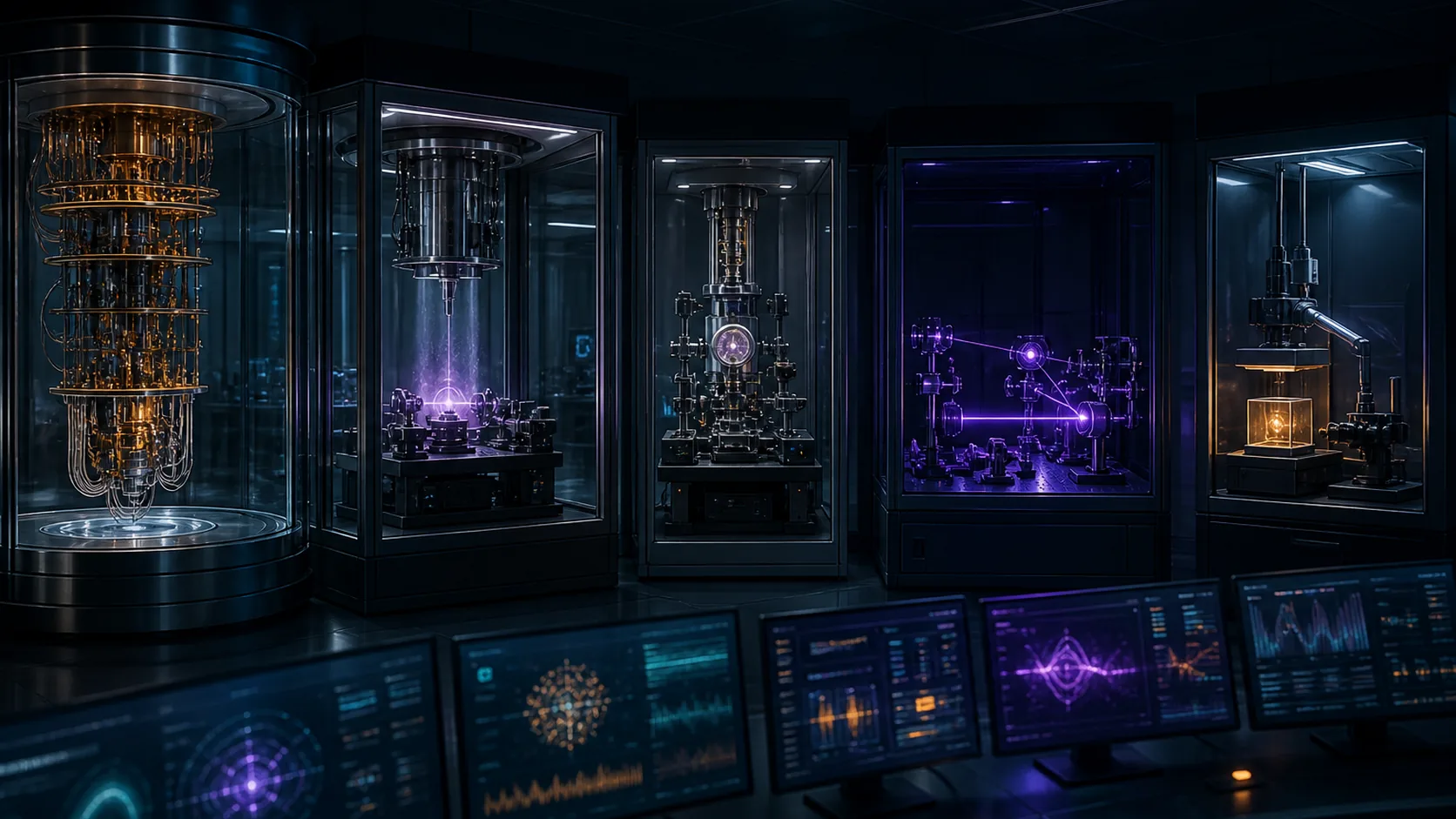
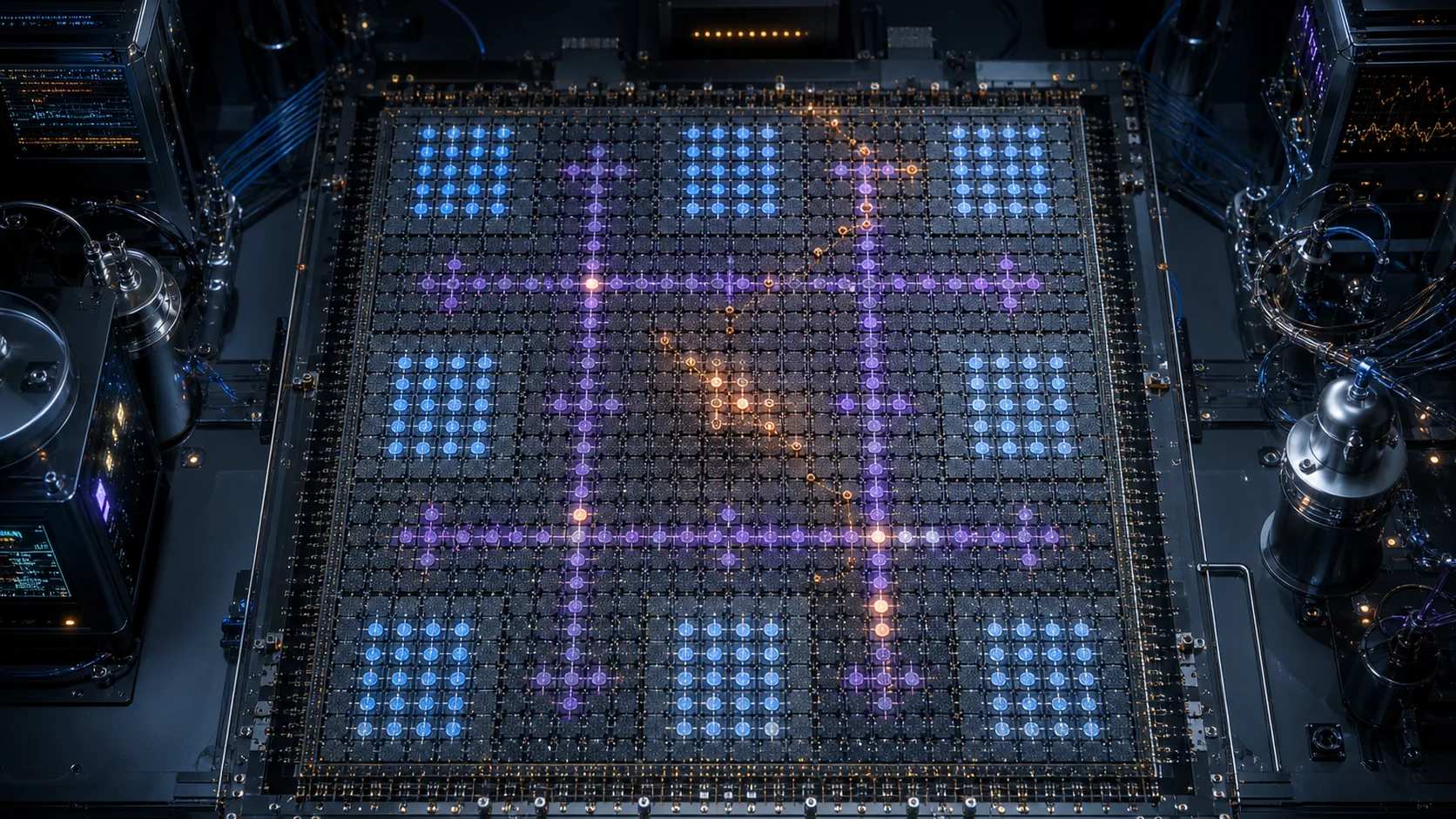
| Criterion | Weight | Rotated surface code | Bivariate bicycle qLDPC | Evidence and interpretation |
|---|---|---|---|---|
| Experimental maturity | 25 | 5 | 2 | Surface-code memory has demonstrated below-threshold scaling through distance 7. The cited BB result is an end-to-end simulation proposal. |
| Hardware connectivity fit | 20 | 5 | 2 | Surface code uses local planar checks. BB requires a degree-6 graph decomposable into two planar edge layers. |
| Memory qubit overhead | 20 | 2 | 5 | The [[144,12,12]] BB code uses 288 total physical qubits for 12 logical memories in the cited design. |
| Logical-gate maturity | 15 | 4 | 2 | Lattice surgery and injection are established surface-code design patterns. Universal BB gate constructions are newer and add ancillas and routing. |
| Decoder maturity and latency | 10 | 5 | 2 | Fast MWPM implementations and real-time demonstrations exist for surface codes. BB decoding remains a development risk. |
| Defect and layout flexibility | 10 | 4 | 2 | Surface-code patches can route around some defects at overhead. BB structure is more sensitive to graph realization. |
| Weighted total | 100 | 415 / 500 | 260 / 500 | Surface code is the production baseline. |
The qLDPC opportunity is real. Bravyi and colleagues estimate that a [[144,12,12]] BB memory can preserve 12 logical qubits for nearly one million syndrome cycles using 288 total physical qubits at 1e-3 physical error, compared with nearly 3,000 physical qubits for comparable surface-code memories. They also require weight-6 checks and degree-6 connectivity made from two edge-disjoint planar subgraphs (Bravyi et al., 2024). That tenfold memory comparison does not yet prove a tenfold saving for universal computation.
Use rotated surface-code patches with lattice surgery for the production path. Maintain a BB qLDPC branch in simulation and on a dedicated test module. Promote BB to production only after it independently passes all of these gates on the selected physical modality:
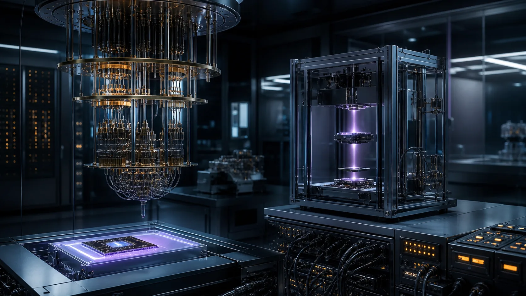
Start with correlated minimum-weight perfect matching (MWPM) using a validated sparse-blossom implementation. At 1e-3 circuit-level depolarizing noise, Sparse Blossom processed both X and Z syndromes for a distance-17 surface-code circuit in less than 1 us per syndrome round on one CPU core (Higgott and Gidney, 2023). Treat that as an algorithm benchmark, not proof of end-to-end controller latency.
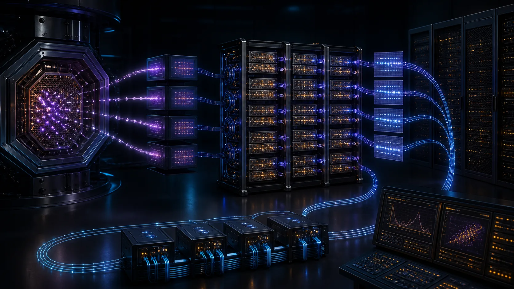
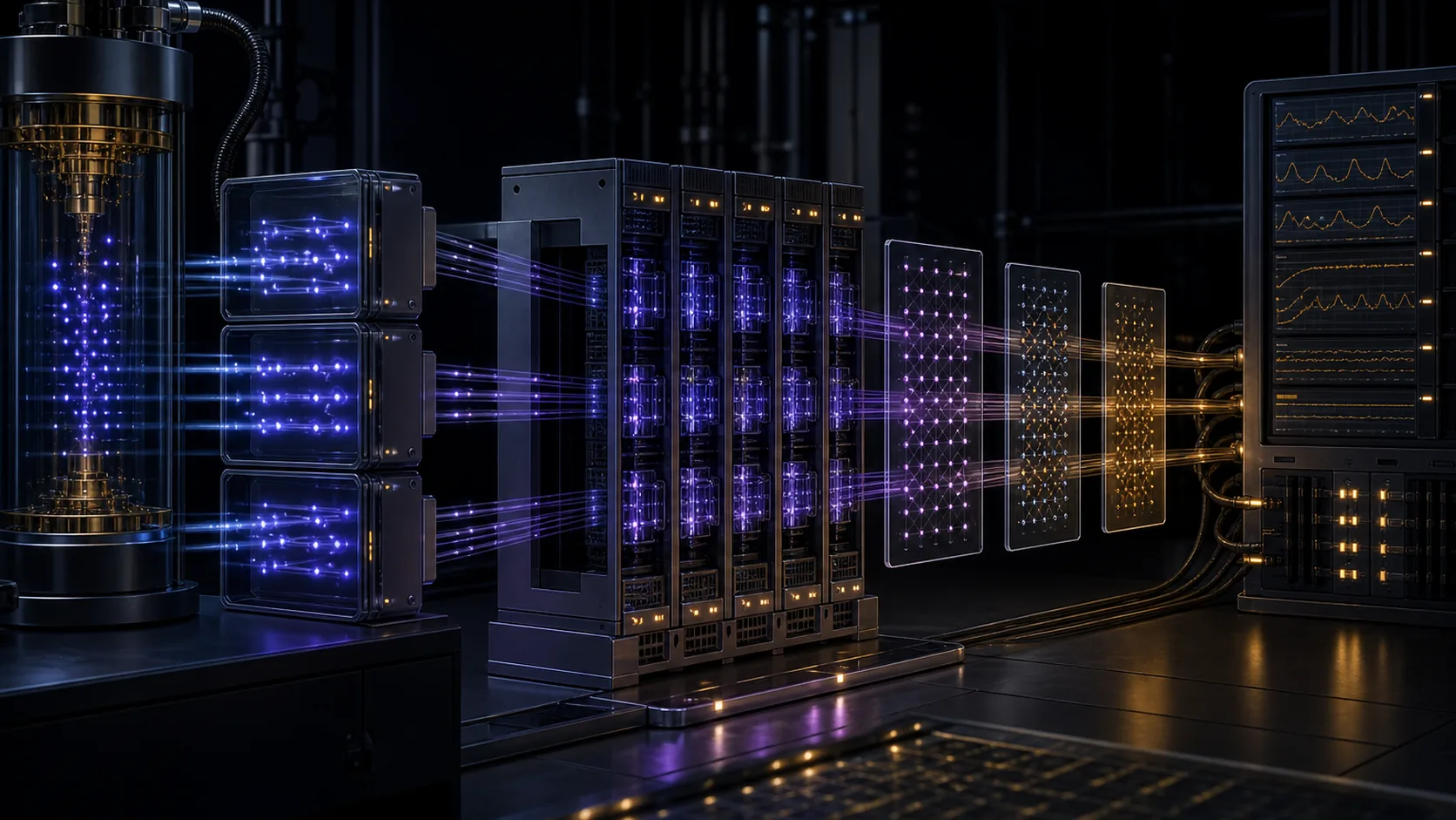
Use two independent decoder paths:
A learned decoder may graduate to the real-time path only after it beats MWPM on held-out hardware data, adversarial drift cases, and rare correlated events, while meeting deterministic latency and versioned-model requirements.
ADC/discriminator -> syndrome bit -> detector event -> local queue -> decoder shard -> Pauli frame -> feed-forward controller
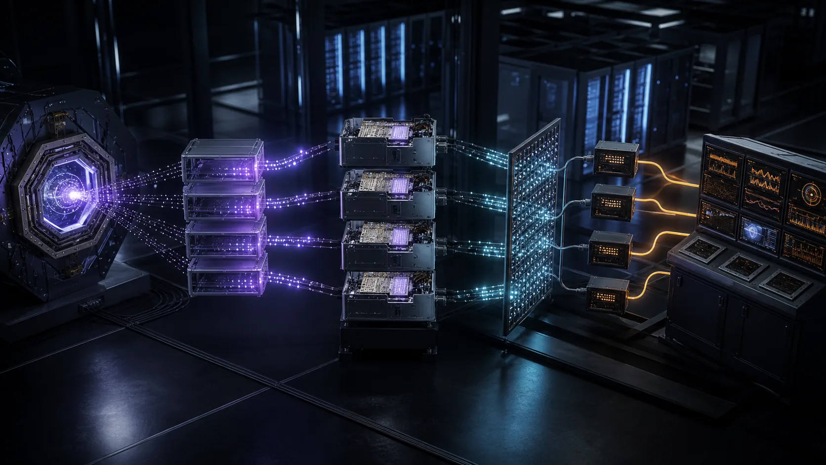
Keep detector extraction next to the readout electronics. Send sparse detector events to decoder shards, not raw ADC traces to a central service. Retain a sampled trace stream for audit and model refitting.
The decoder service-level objectives are engineering targets:
| Metric | Acceptance target |
|---|---|
| Sustained processing | At least one complete syndrome round per 1 us cycle per assigned shard |
| Utilization at nominal load | <= 50 percent to retain burst margin |
| Queue growth | Zero monotonic growth over 1e6 continuous cycles |
| Feed-forward reaction | p99.9 <= 10 us from final required measurement to controller-visible decision |
| Frame loss or duplication | Zero in fault-injection tests; sequence numbers must detect both |
| Real-time versus audit logical result | Statistically consistent on held-out shots, with every mismatch retained and classified |
Published demonstrations show both progress and the remaining gap. An FPGA-integrated decoder reported mean decoding below 1 us per round and 9.6 us response after nine rounds (Caune et al., 2024). Google reported average final-decoder latency of 63 us for distance 5 over runs as long as one million cycles (Acharya et al., 2024). The program's 10 us reaction target is therefore aggressive but grounded, and it must be measured end to end.
Model arrival and service distributions from detector-event data, including bursts. Average throughput alone is insufficient because a decoder can appear fast while its tail creates an unbounded queue. For each code distance and noise regime, publish the queue-depth distribution, p99.9 latency, maximum observed latency, and recovery time after injected bursts.
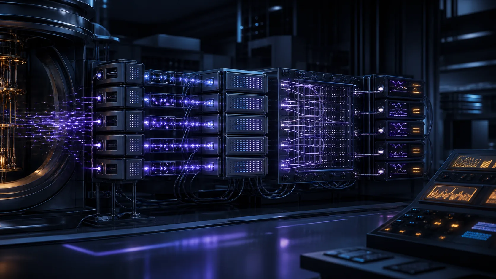
If a Pauli-frame update is late but no non-Clifford feed-forward boundary has been reached, continue syndrome extraction while retaining order. If a hard feed-forward deadline will be missed, enter a syndrome-safe hold when the hardware supports it; otherwise abort the shot, mark it invalid, preserve the trace, and return an explicit runtime error. Never substitute a stale frame or silently drop a syndrome.
Current demonstrations support feasibility anchors, not a defensible installed-power or capital quote. A Collision Clustering ASIC design was reported at 0.06 mm^2 and 8 mW while simulating megahertz decoding for a surface-code memory of up to 1,057 physical qubits (Liyanage et al., 2025). A naive linear projection is about 7.6 W of decoder-core power per million physical qubits, but it excludes detector extraction, input and output, memory, network fabric, hosts, redundancy, the audit decoder, power conversion, and cooling. It is therefore a research anchor, not an installed-power estimate. An FPGA local-clustering implementation used less than 10 percent of a high-end device for a distance-17 patch in simulation, but likewise does not close whole-system power or cost (Smith et al., 2025).
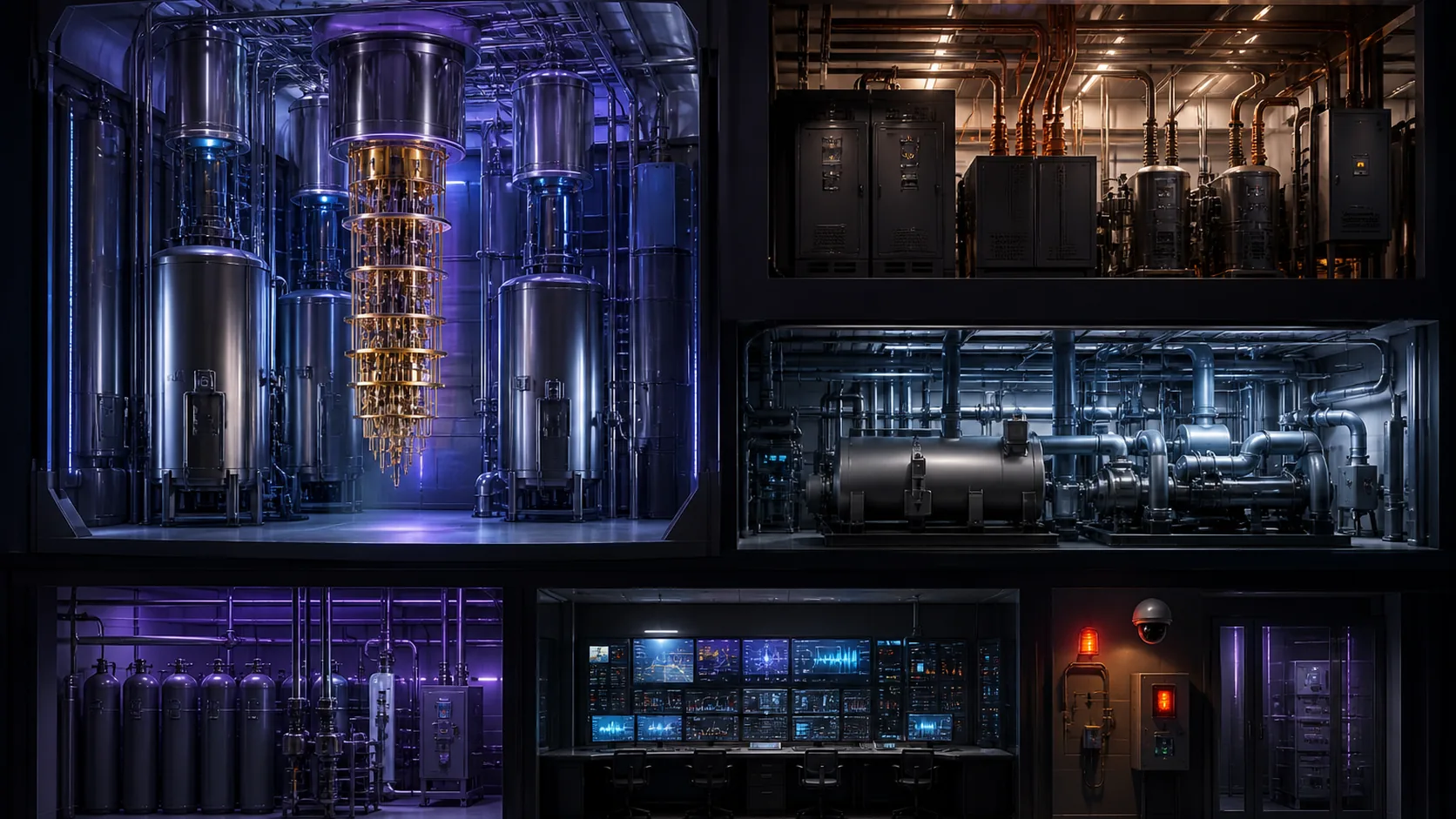
Size the production service from measured detector-event traffic. If R_peak is the burst-conditioned event rate and one validated shard sustains r_shard while meeting the latency target, use
N_shards = ceil(2 R_peak / r_shard) + N_spare
where the factor of two enforces the 50 percent utilization ceiling. Compute installed power and capital from the selected bills of material:
P_installed = sum(N_i P_i) + P_network + P_storage + P_audit + P_cooling
C_installed = sum(N_i C_i) + C_network + C_storage + C_integration + C_spares
Before freezing either number, operate a decoder service at no less than one percent of the next phase's syndrome load using representative distance, surgery, physical error, leakage, and burst traces. Measure power at the facility feed, obtain dated vendor quotes, project low, base, and high cases, and repeat the end-to-end latency and backlog tests after a shard failure. Until that gate passes, any fixed decoder dollar or megawatt line is a separately identified facility reservation or management contingency, not a validated decoder estimate and not part of a precise baseline total.
Clifford operations alone are not universal. The baseline universal path consumes injected T or CCZ resource states, with a factory design selected by phase.
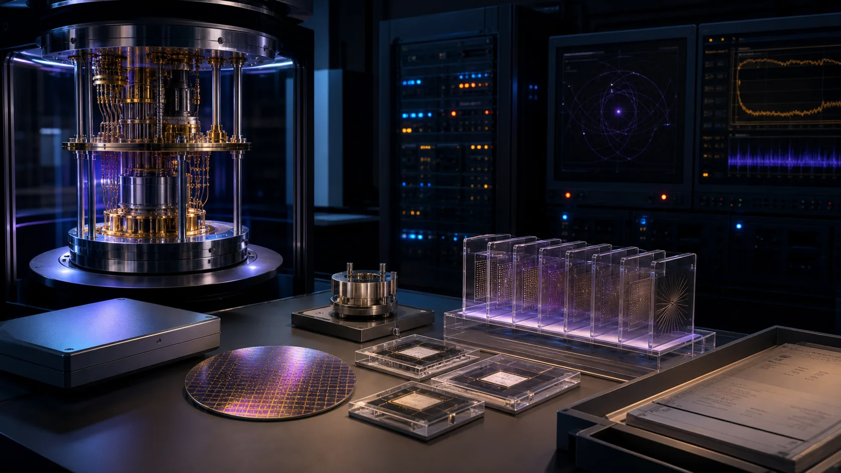
8T-to-CCZ distillation. Cultivation simulations report T-state error as low as 2e-9 at 1e-3 uniform circuit noise, with roughly an order-of-magnitude lower qubit-round cost than earlier approaches (Gidney, Shutty, and Jones, 2024). A later superconducting-processor preprint experimentally reported state fidelity 0.9999(1) while retaining 8 percent of attempts, which is promising but also exposes a yield and throughput risk (Rosenfeld et al., 2025).For the mission configuration, set cultivated T-state error to at most 1e-7 and apply 8T-to-CCZ suppression. The RSA design uses the approximation 28p^2, so p = 1e-7 gives CCZ error below 1e-12 (Gidney, 2025). Verify the actual factory under the measured, correlated device noise before relying on this equation.
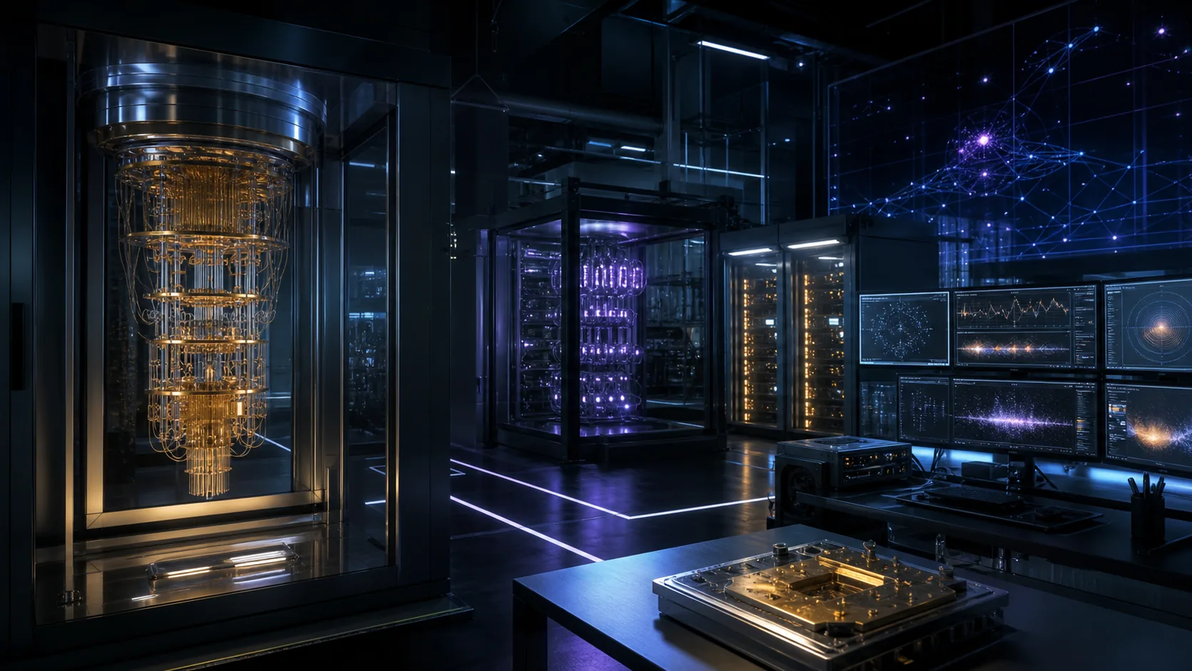
For a compiled schedule, size the number of factories using
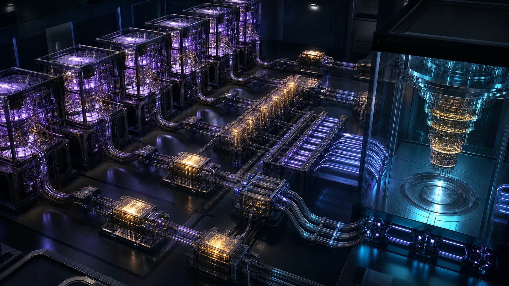
factories >= ceil(required_CCZ_rate / validated_factory_rate * margin)
where the margin covers heralded rejection, maintenance, routing stalls, and drift. Do not size from nominal cycle time alone.
The 2025 RSA layout uses six factories, budgets 150 code rounds per accepted CCZ across the bank, and therefore supplies one CCZ every 25 us at distance 25 with a 1 us code cycle. The target workloads in B5 consume about 15,000 Toffolis per second on average, while this cited six-factory layout is budgeted for about 40,000 CCZ states per second. Those are derived average rates; burst demand and circuit dependency depth still require schedule simulation.
Every factory must expose accepted and rejected attempts, inferred output error, input calibration identifiers, decoder version, and buffer age. A factory that falls outside its validated yield or error envelope is quarantined automatically, with the application rescheduled or failed explicitly.
These are architectural north stars, not first-release promises. Reproduce each source's calculation and rerun the resource estimator whenever the algorithm, code, error model, cycle time, or factory changes.
| Target | Published logical workload | Non-Clifford count | Published physical estimate and runtime | What the number means |
|---|---|---|---|---|
| FeMoco active-space ground-state energy by tensor hypercontraction and qubitization | 2,142 logical qubits | 5.3e9 Toffolis. Selected 8T-to-CCZ factory mapping would consume up to 4.24e10 cultivated T candidates before rejection and buffering. | About 4 million physical qubits and under 4 days at 1 us cycles and physical error no worse than 1e-3 | Published full-stack estimate from Lee et al., 2021. It targets a specific active-space Hamiltonian, not all nitrogenase chemistry. |
| RSA-2048 factoring by approximate-residue period finding | 1,399 algorithmic logical qubits at the highlighted point; 1,537 including idle hot tiles in the physical layout | 6.5e9 expected Toffolis. The same factory mapping corresponds to 5.2e10 cultivated T candidates before rejection and buffering. | 897,864 calculated physical qubits, reported with slack as fewer than 1 million; 4.96 expected days, reported with slack as under one week | Published estimate from Gidney, 2025, assuming 1e-3 uniform noise, 1 us cycles, 10 us reaction, and nearest-neighbor planar qubits. |
The FeMoco raw logical-data footprint at the distance-25 active-tile allowance is a derived 2,142 * 1,352 = 2,895,984 physical qubits. Factories, routing, and workspace bring the cited plan to about four million. Its average Toffoli demand is a derived 5.3e9 / (4 days) = 15,336 per second.
The RSA physical arithmetic is independently reproducible from the cited layout:
1,280 cold logicals 430 + 131 hot logicals 1,352 + 170,352 compute qubits = 897,864 physical qubits
Its average Toffoli demand is a derived 6.5e9 / 4.96 days = 15,168 per second. The cold-storage density relies on yoked surface codes and remains a study assumption with workload details left open by the author. Keep one million as the planning floor, not a procurement promise.
Move through these logical capability gates. Physical counts are deliberately ranges until Part A closes yield, packaging, and control density.
| Gate | Required capability | Exit proof |
|---|---|---|
| L0 | Compiler, scheduler, noise model, decoder, and resource estimator in simulation | Reproduce published small-code curves and both B5 arithmetic baselines from immutable inputs. |
| L1 | Physical characterization and repetition codes | Stable repeated syndrome extraction, leakage removal, and correlated-error map. |
| L2 | Distance-3, distance-5, and distance-7 surface-code memories | Lambda > 1 with confidence bounds on the same module and no observed floor over the tested duration. |
| L3 | Two logical qubits with Clifford operations and lattice surgery | Logical randomized and cycle benchmarks beat the corresponding unencoded operation. |
| L4 | Injected non-Clifford operation | End-to-end logical T or CCZ result, including real-time feed-forward, beats an unencoded implementation. |
| L5 | Small fault-tolerant application | Known factoring and chemistry outputs pass the user workflows in B7. |
| L6 | Factory bank plus hundreds of logical qubits | Sustained factory, decoder, and calibration service with restart and fault recovery. |
| L7 | Mission scale | A fresh estimator run, hardware evidence, and staged rehearsal justify the million-scale or multi-million-scale build. |
| Layer | Responsibilities | Required artifact |
|---|---|---|
| User and workflow | Python APIs, chemistry and cryptanalysis workflows, job intent, result interpretation | Versioned job bundle with inputs, requested accuracy, and success criteria |
| Language interchange | Dynamic circuits, classical control, timing intent, calibration hooks | OpenQASM 3 input and output; its specification covers real-time classical control, explicit timing, and pulse-level calibration (OpenQASM specification) |
| Compiler intermediate representation | Hardware-independent quantum and classical control flow, target lowering, optimization passes | QIR or a typed MLIR dialect with a documented lowering contract; QIR is maintained as an interoperability effort by the QIR Alliance |
| Fault-tolerant compiler | Clifford and non-Clifford decomposition, rotation synthesis, code-distance assignment, lattice surgery, factory allocation, routing | Logical instruction graph, error ledger, and physical schedule |
| Resource estimator | Space, time, bandwidth, energy, failure probability, and sensitivity sweeps | Machine-readable estimate plus assumptions and uncertainty ranges |
| Runtime orchestrator | Admission control, calibration validity, module reservation, checkpoint policy, result assembly | Immutable execution manifest and event log |
| Real-time control | Pulse microcode, measurement discrimination, detector extraction, decoding, Pauli frame, feed-forward | Bounded-latency controller image with trace identifiers |
| Calibration service | Device graph, parameter store, experiment planner, drift detector, rollback | Signed calibration snapshot with validity window and dependency graph |
| Simulation and verification | Stabilizer simulation, noisy Monte Carlo, decoder comparison, small exact simulation | Reproducible test corpus and golden outputs |
| HPC integration | Hamiltonian generation, integral factorization, circuit generation, classical post-processing, decoder training | Content-addressed datasets and provenance graph |
Use Stim for high-throughput stabilizer and detector-error-model testing; it can sample large stabilizer circuits efficiently and is designed for QEC workloads (Gidney, 2021). Use PyMatching or an independently validated sparse-blossom implementation for the baseline decoder. Pin exact versions at each phase gate, but avoid freezing product choices in this plan before benchmark and licensing review.
Every lowering pass shall emit a checkable equivalence witness or be covered by property tests and differential simulation. The pipeline shall preserve:
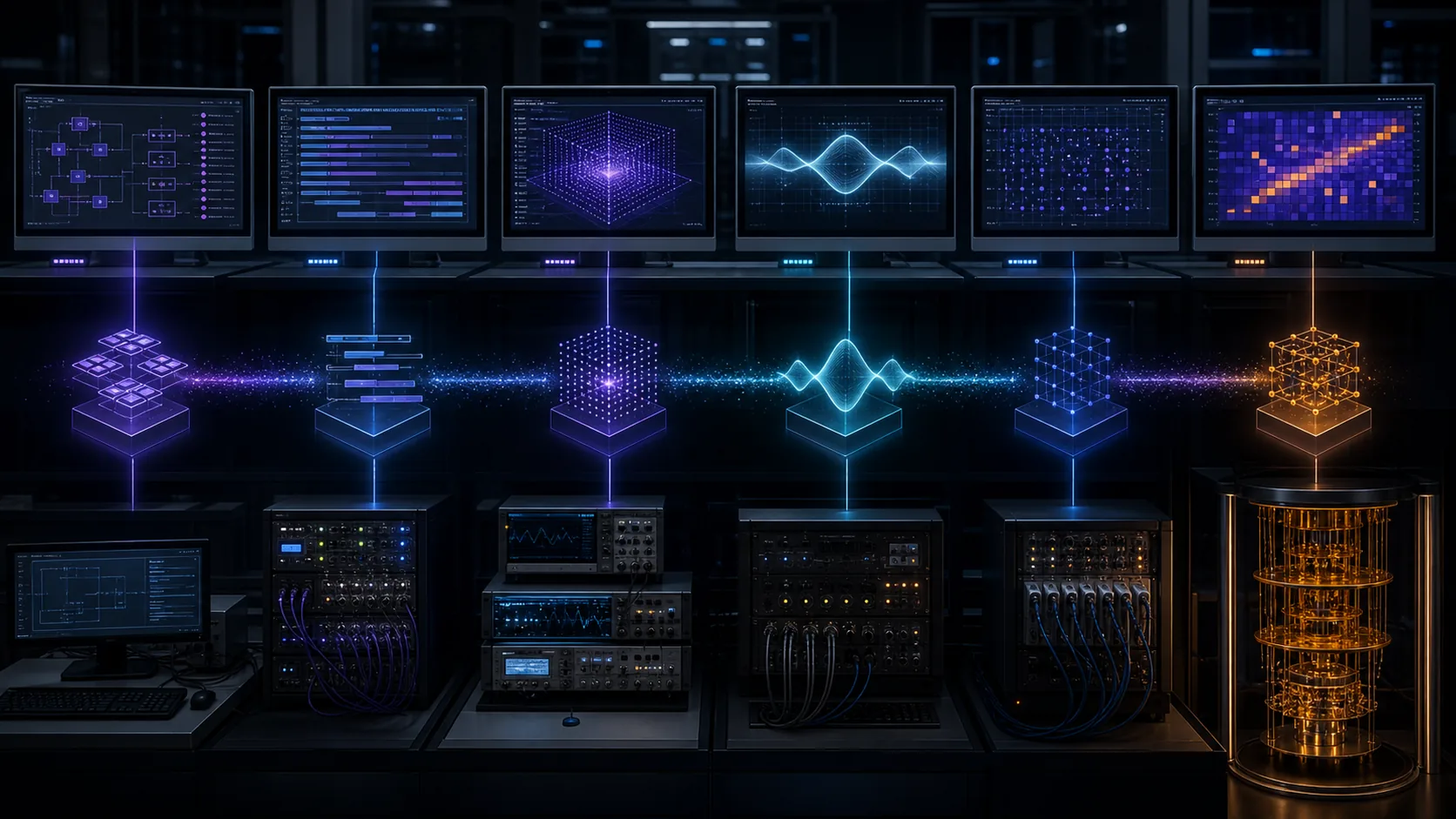
For circuits small enough to simulate exactly, compare the compiled distribution with an independent simulator. For larger Clifford regions, use stabilizer equivalence. For non-Clifford regions, use cut points, tensor or decision-diagram checks where feasible, algebraic identities, and randomized differential tests. A compiler mismatch blocks hardware execution.
The runtime accepts a job only when its calibration snapshot is valid for every physical operation in the schedule and its predicted failure budget passes. It shall refuse, rather than silently approximate, unsupported dynamic control, expired calibrations, missing channels, insufficient factory capacity, or a decoder configuration that cannot meet the latency envelope.
Store enough provenance to replay a result: source program hash, compiler and pass versions, target topology, calibration snapshot, pulse and controller images, decoder binary and weight set, resource-state batches, timestamps, environmental alarms, raw counts, syndrome summary, and result post-processing version.
Calibration is a closed loop. Fast canaries monitor readout, selected gates, leakage, and detector statistics between jobs. A drift alarm invalidates dependent calibrations, drains new jobs, and either recalibrates or rolls back. Long jobs use predeclared safe checkpoints; never splice incompatible calibration regimes without marking a new execution segment in the error ledger.
Admission control places a job only on healthy regions and leaves declared spare capacity. Losing a module or cryostat during a job is not transparent: the runtime may migrate a logical state only through a tested fault-tolerant protocol with budgeted link operations. Otherwise it must reach a syndrome-safe checkpoint, abort the affected execution segment, and restart from a verified checkpoint or from the beginning. Recompiling around an offline region is valid only before state placement or after such a restart.
A build, type check, process launch, green status, HTTP success, unit test, or short smoke run proves only that check. Machine acceptance requires the representative workflow to produce the expected quantum output, state change, persistence, and recovery behavior.
Use randomized benchmarking for average physical gate error (Magesan, Gambetta, and Emerson, 2011), simultaneous randomized benchmarking for addressability, and cycle benchmarking for multi-qubit layer error and crosstalk (Erhard et al., 2019). These characterize components. They do not replace logical memory, logical gate, decoder, and application tests.
| Phase | Representative input | Required observation | Negative and boundary checks |
|---|---|---|---|
| Digital model | Published distance-3 through distance-17 circuits under declared circuit noise | Reproduced logical-error curves within Monte Carlo confidence intervals; two decoders agree on sampled cases | Corrupt detector graph, wrong boundary, correlated burst, and decoder timeout must be detected |
| Physical primitives | Randomized and simultaneous gate sequences across the full module | Median and tail errors meet B1; leakage, readout confusion, and crosstalk are separately reported | Run at calibration-window edges, maximum parallelism, thermal transients, and disabled channels |
| Repeated QEC | Distance 3, 5, and 7 using the same cycle and comparable regions | Logical error decreases with distance with lower confidence bound Lambda > 1; logical lifetime exceeds best constituent physical lifetime | Disable leakage removal, inject coherent errors, drift selected qubits, and inject lost syndrome frames |
| Decoder | 1e6 continuous syndrome cycles plus recorded and synthetic bursts | No queue growth, p99.9 reaction within B3 target, real-time result agrees statistically with audit decoder | Saturate event rate, delay packets, duplicate sequence numbers, restart one shard, and corrupt model weights |
| Logical Clifford | Prepared logical basis and randomized logical Clifford sequences | Logical gate error is measured directly and beats the comparable unencoded operation | Wrong Pauli frame, surgery-boundary defect, stale calibration, and mid-sequence restart |
| Non-Clifford | Injected T and CCZ states with heralding and feed-forward | Output fidelity and accepted-state throughput meet the compiled job budget | Factory rejection burst, stale buffered state, failed feed-forward, and one factory quarantined |
| Small factoring workflow | Compile and run period finding for a classically known small composite such as 15 or 21 | Returned samples lead through the same post-processing path to valid nontrivial factors; persisted result can be independently replayed | Prime input, unlucky sample requiring retry, invalid program, decoder overload, and process restart |
| Small chemistry workflow | H2 or another exactly checkable active-space Hamiltonian, geometry and precision fixed in the job bundle | Energy and uncertainty agree with an independent exact diagonalization within the requested tolerance | Bad integral hash, insufficient precision budget, state-preparation failure, and expired calibration |
| Mission rehearsal | Scaled trace replay for FeMoco and RSA schedules with measured service distributions | Resource, queue, factory, checkpoint, and error budgets close with sensitivity ranges and reserve | Worst credible drift, factory loss, module loss, radiation burst, storage corruption, and recovery from checkpoint |
Pre-register the metric, shot count, confidence level, exclusion rules, and stopping rule. Report confidence intervals and all tried variants, not only the best device region. Keep a holdout interval of hardware data for decoder and noise-model validation.
When zero failures are observed in N independent opportunities, the approximate one-sided 95 percent upper bound is 3/N. This means direct demonstration of a 1e-15 rate would require an impractical number of independent trials. Mission confidence must therefore combine lower-distance scaling, targeted accelerated tests of rare mechanisms, validated physical models, redundancy, and conservative reserve. Label the resulting 1e-15 figure as extrapolated until direct evidence exists.
The machine is functionally useful only when an external user can submit a versioned job, receive an interpretable result with uncertainty and provenance, replay its classical processing, and see explicit failure when any prerequisite is not met. For each major phase, independently reproduce at least one end-to-end workflow after a cold controller restart and after restoring the calibration database from its persisted state.
| Risk | Likelihood / impact | Leading indicator | Mitigation and decision trigger | Owner |
|---|---|---|---|---|
| Correlated error floor defeats distance scaling | High / critical | Lambda degrades with distance or long runs show burst clusters | Radiation shielding, gap engineering, leakage removal, spatial isolation, burst-aware decoding. Stop scale-up if the measured floor misses the next phase budget. | QEC and device physics |
| Decoder backlog | Medium / critical | Queue tail grows during bursts or simultaneous surgery | Shard locally, overprovision to at most 50 percent nominal utilization, use hardware acceleration, and add safe holds. Block logical non-Clifford work if p99.9 reaction misses 10 us. | Real-time systems |
| Decoder model mismatch | High / high | Audit decoder outperforms production or mismatch rate drifts | Online detector statistics, scheduled refits, held-out validation, version rollback, and dual decoding. | QEC software |
| Calibration drift during long jobs | High / high | Canary changes, detector-rate shift, or rising factory rejection | Dependency-aware invalidation, checkpoints, redundant modules, and explicit segment boundaries. Abort rather than mix untracked regimes. | Calibration |
| Compiler or scheduler miscompilation | Medium / critical | Differential simulation mismatch or observable-map inconsistency | Verified passes where feasible, property tests, independent simulator, immutable manifests, and staged canaries. Any unexplained mismatch blocks release. | Compiler |
| Magic-state yield or fidelity misses plan | High / critical | Rejection rate, buffer age, or output-error bound exceeds envelope | Keep conventional distillation fallback, add factories, improve physical noise, or reschedule. Do not borrow from job failure reserve without review. | Fault-tolerant architecture |
| qLDPC savings vanish in full computation | High / medium | Couplers, ancillas, decoder, and gate routing erase memory advantage | Keep qLDPC behind the B2 upgrade gate and compare compiled applications, not code rate alone. | Architecture research |
| Resource estimate becomes stale | High / high | Algorithm, error model, or factory revision changes key inputs | Machine-readable estimator in continuous integration; rerun sensitivity sweeps at every phase gate. | Algorithms and systems |
| Rare failure cannot be statistically bounded | High / critical | Zero-event bound remains far above mission target | Accelerated environmental tests, physics-based hazard model, redundancy, error-detecting job checks, and conservative uncertainty. Label extrapolation. | Reliability |
| Provenance or result data is incomplete | Medium / high | Replay cannot reconstruct a run | Content-address all inputs and controller artifacts, validate schemas before admission, replicate storage, and test restore. | Runtime and data |
| Classical bandwidth or power exceeds facility plan | Medium / critical | Per-module event rate, decoder power, or network utilization exceeds envelope | Edge detector extraction, sparse events, hierarchical aggregation, ASIC path, and phase-gate power budgets. | Controls and facilities |
| Application model is scientifically inadequate | Medium / high | Chemistry active space or cryptanalytic assumptions fail external review | Treat algorithm input construction as a peer-reviewed work product, compare alternative models, and state scope. Hardware success does not validate the scientific model. | Applications |
The risk register is reviewed at every scale gate. A risk closes only with observed evidence against its trigger, not because a mitigation task was scheduled.
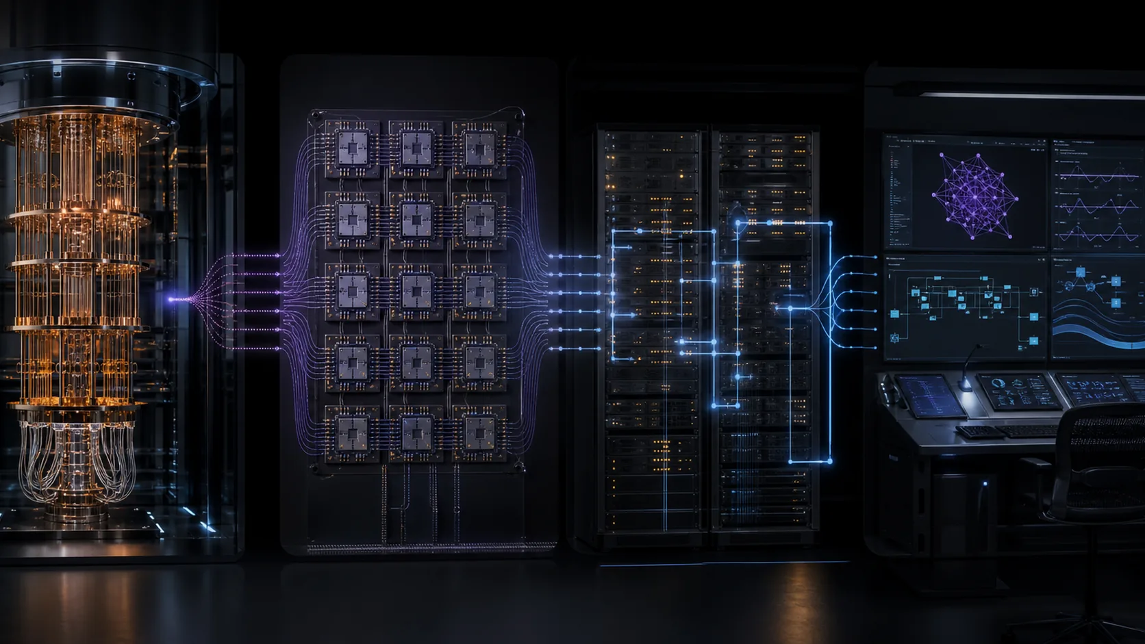
Written jointly. Part A owns the hardware side of each row, Part B owns the logical side. Where the two authors disagreed, the resolution and the reason are recorded rather than smoothed over.
These are the numbers both halves are built against. Where Part A's first draft differed, Part B's value was adopted and the reason is given.
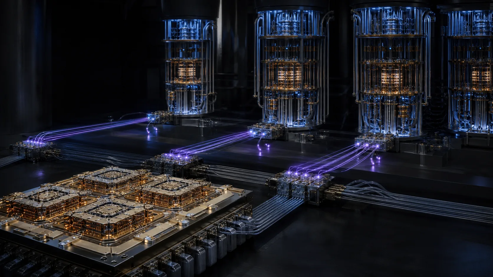
| Quantity | Agreed value | Origin | Resolution |
|---|---|---|---|
| Median one-qubit error | <= 1e-4 | B1.2 | agreed on both sides from the start |
| 95th-percentile two-qubit error | <= 1e-3, stretch 5e-4 | B1.2 | agreed; matches the uniform 1e-3 assumption in the published resource estimates [SRC] |
| Measurement plus reset error | <= 1e-3 per measured ancilla | B1.2 | Part A corrected from 5e-3. Part B's value is better justified. Hardware consequence: commodity readout is 2.5e-2 today, so this is a 25x improvement requirement |
| Measurement plus reset time | <= 600 ns | B1.2 | Part A corrected from 1.0 us. Frees 8.4 us of decoder budget instead of 8 us |
| QEC cycle time | 1 us, 1.1 us acceptable at first below-threshold gate | B1.2 and A1.3 | agreed |
| Feed-forward reaction | <= 10 us at p99.9 | B1.2 | agreed, but see J3: measured practice is 63 us |
| Logical memory error, hot patch | <= 1e-15 per logical-qubit round | B1.2 | Part A corrected. Its draft had a single 1e-9 figure conflating three quantities |
| Non-Clifford resource error | <= 1e-12 per consumed CCZ | B1.2 | Part A corrected |
| Cultivated T-state error | <= 1e-7 before 8T-to-CCZ | B4.1 | Part A corrected |
| Physical qubits per active logical tile, d=25 | 1,352, from 2(d+1)^2 | B1.4 | Part A corrected from 1,249. 2d^2-1 is the raw memory patch; active lattice surgery needs the larger figure |
| Control addressability | 2 scheduled actuation degrees per tunable qubit, 1 result per syndrome ancilla | B1.2 | agreed. Part B explicitly permits Part A to multiplex physical lines, which is what makes CRY-1 legal |
| Syndrome output | ~0.5 bit per physical qubit per cycle | B1.2 | agreed. 0.66 Tb/s at Part A's 1,310,720 qubits [EST] |
| Detector extraction location | at the readout electronics, sparse events only | B3.2 | agreed, and Part A now treats this as a hard requirement on the cryo-CMOS die, not a software preference. Centralized export of 0.66 Tb/s is not buildable |
| Qubit lattice topology | UNRESOLVED | A3.4 | Part B's resource estimates assume one square nearest-neighbor grid, per their source. Part A specifies 20 cryostats joined by links. The two halves are not currently built against the same topology, and no runtime or resource figure crossing that boundary should be treated as settled until LNK-1 closes |
Recomputed independently in verify/part-b-arithmetic-check.py.
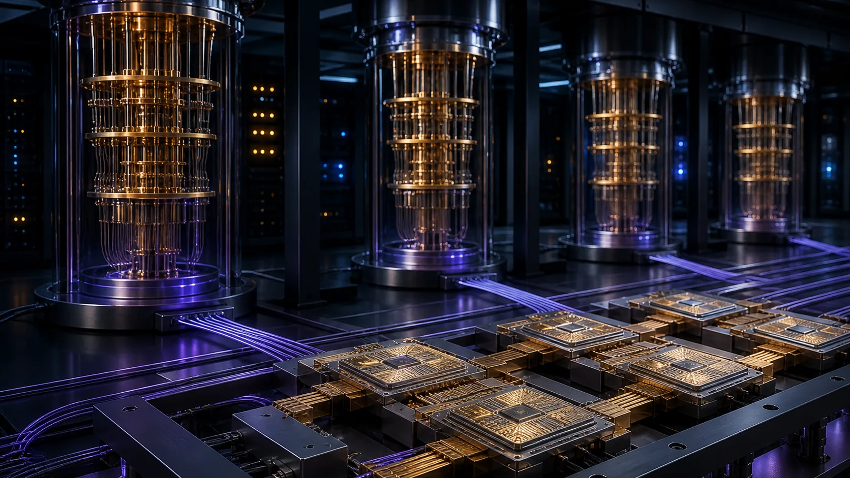
| Workload | Physical qubits required | Phase 3 machine, 1,310,720 |
|---|---|---|
| RSA-2048, Gidney 2025 layout | 897,864, reconstructed as 1,280 x 430 + 131 x 1,352 + 170,352 | fits on qubit count, 46 percent margin |
| FeMoco, Lee et al. full stack | ~4,000,000 | short by 2,689,280, needs 3.05x |
| FeMoco, optimistic 1,137-logical variant | 1,537,224 data qubits before factories and routing | does not fit |
Gate 3 was rescoped accordingly: RSA-2048 plus a chemistry problem sized to the machine. Phase 4 closes the FeMoco gap at $3.8B incremental and is deliberately not baselined, on the reasoning in A8.2.
Read the RSA row narrowly. It says the qubit count fits. It does not say the workload runs in the published time, because both the count and the 4.96 day runtime come from a source assuming a single square nearest-neighbor grid, and this machine is 20 linked cryostats. The qubit-count margin is real; the runtime is unresolved (A3.4, J3 item 1). Those two facts are easy to conflate and the earlier draft conflated them.
These are unresolved. They are listed here rather than buried so that a reader does not have to discover them.
| Item | Raised by | Resolution |
|---|---|---|
| B2.1 weighted total stated as 440 | Claude Code | Fixed by Codex. Recomputation from his own weights and scores gives 415. Decision unchanged: 415 against 260 still selects the surface code |
| Defect tolerance per patch unspecified | Claude Code | Answered by reasoned refusal. B1.4 declines to convert a bare yield percentage into logical capacity and requires a measured defect map plus layout Monte Carlo, because clustered defects and frequency collisions break the independence assumption in Part A's yield table. Part A's FAB-1 is now explicitly labelled unjustified rather than carrying a false number |
| Decoder capital and power unsized | Claude Code | Answered by reasoned refusal plus an anchor. B3.4 gives 7.6 W of decoder-core power per million physical qubits (independently recomputed as 7.57 W) and a closure gate, while declining to issue an installed-power or capital figure. Part A's $200M is reclassified from estimate to facility reservation |
| Graceful degradation on cluster loss | Claude Code | Answered, and Part A's framing corrected. B6.3 establishes that mid-job module loss is not transparent and that recompiling around an offline region is valid only before state placement or after a restart. This surfaced three previously uncaptured hardware requirements in A7, all unpriced |
| Four interface value conflicts | both | Resolved, all four in Part B's favour. See J1 |
| Gate 3 claimed a workload the machine cannot run | Claude Code | Rescoped. See J2 |
Both review passes are now complete: Claude Code reviewed Part B and Codex acted on it; Codex reviewed Part A and Claude Code acted on it (A10.1). What follows survived both passes.
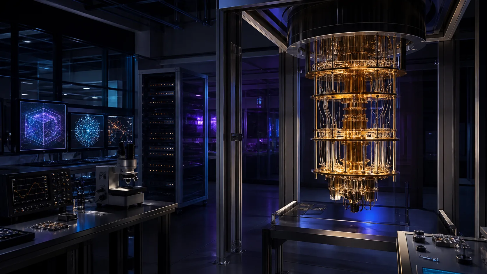
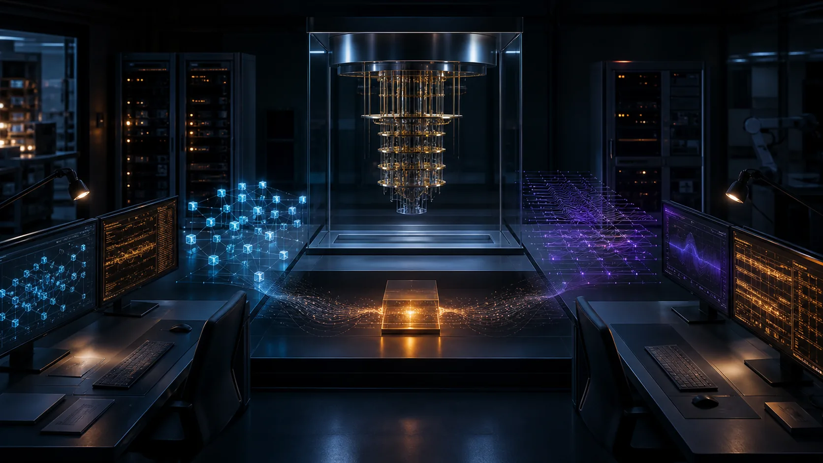
| # | Item | Owner | Why it matters |
|---|---|---|---|
| 1 | LNK-1: the distributed-overhead multiplier is unmeasured | both, A3.4 | The largest single hole. The RSA estimate assumes one square nearest-neighbor grid; this is a 20-cryostat machine. A multiplier of 1.41 erases the whole margin to 7 days. Closure needs Codex's estimator run against the real connectivity graph, not a square lattice |
| 2 | The 4 K budget is not closed, and the two published cryo-CMOS cases differ by 13.75x | Claude Code, A5.4 | Straddles buildability (3.1 W vs 43.3 W per cryostat) and drives the entire $1.8B to $6.1B cost range. Highest-value research item in the programme |
| 3 | H13: the 10 us reaction budget versus 63 us measured practice | both | Tied for highest exposure. Undercuts the clock-speed argument that selected the modality |
| 4 | No like-for-like modality comparison exists | both, A2.3 | The 676x figure was withdrawn as invalid. Neither superconducting nor neutral atom has been evaluated at equal workload and equal logical reliability on spacetime volume and energy. The 385-to-380 score is weaker than it looks |
| 5 | FAB-1 is unjustified | Claude Code, Phase 1 | Part A cannot presently defend its own fab yield spec. Closure requires the measured defect map and layout Monte Carlo specified in B1.4 |
| 6 | Decoder installed power and capital are reservations | Codex, B3.4 gate | The $200M sits inside the base-case total so it is not understated, but it is not validated |
| 7 | Seam equivalence is unmeasured | Claude Code, A3.1 | Until measured, no seam-spanning mission layout is justified, which is why module size is now a gated variable rather than fixed at 1,024 |
| 8 | The 20 mK stage has never been budgeted | Claude Code, H17 | KIDE gives > 90 uW at 20 mK, about 1.4 nW per qubit at this plan's density. Nothing has been costed against it |
| 9 | Checkpoint storage and maintenance-window spare capacity are unpriced | Claude Code | A 4.96 day run needs a five-day no-touch guarantee across 20 cryostats, and the state has to be checkpointed somewhere physical |
What was actually exercised, with what inputs, and what was observed.
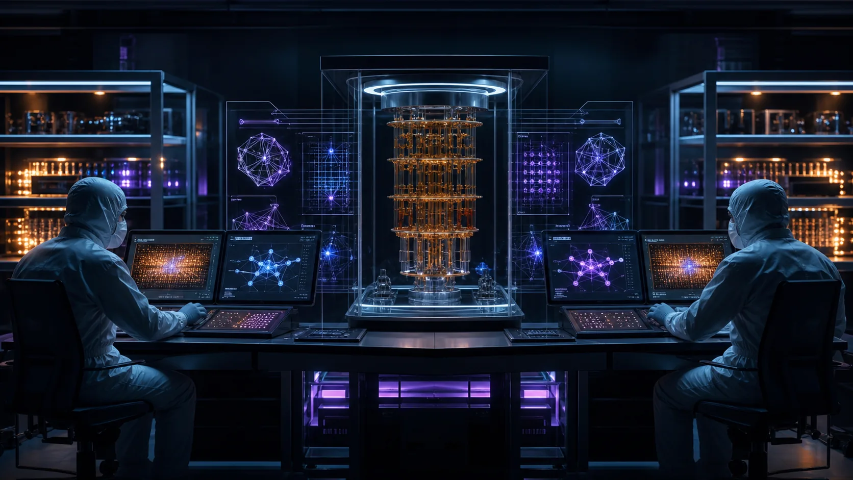
Part A, checked by its own author. verify/part-a-arithmetic-check.py, 108 assertions covering the trade-study weighted totals, the thermal and wiring derivations, the scaling tiers, the yield model, the full capital breakdown, the staffing tables, the clock-speed scaling table, the latency split, and every figure arising from Codex's cross-review: the KIDE vendor comparison, the phase-gate patch sizes, the 4 K per-channel cases, the distributed-overhead sensitivity table, and the three cost cases. Current result: 108 pass, 0 fail.
The first run failed 4 of 58, all in the cost table: contingency stated as $144M against a computed $338M, Phase 3 total stated as $2.4B against $2.6B, program capex stated as $4.1B against $3.0B, and a claimed 60 percent cost share that was actually 40 percent. All four corrected. Fixing the last one is what surfaced the 7-percent-qubit-cost finding in the executive summary.
The limit of this checker, stated plainly. It passed 73 of 73 on a version of Part A that contained an unsupported RSA runtime claim, a phase gate whose device was too small to run it, an uncosted 4 K stage, an invalid 676x comparison, and a cryostat count 65.5x beyond vendor scale. Every one of those was arithmetically sound and premised on something nobody had checked. A passing arithmetic checker is evidence about arithmetic and nothing else, and reporting it as though it were evidence about correctness would have been the single most misleading thing in this document.
Part B, checked by Part A's author. verify/part-b-arithmetic-check.py, 28 assertions. Each recomputes from Codex's cited inputs rather than reading his stated results. Independently reproduced: all ten patch and tile sizes in B1.4; the 0.5 Tb/s syndrome aggregate; the 0.0065 union bound; the 28p^2 suppression to 2.8e-13; the six-factory bank at one CCZ per 25 us and 40,000 CCZ/s; the RSA layout reconstruction to the exact qubit (897,864); both Toffoli demand rates (15,168/s and 15,336/s); both 8T-to-CCZ candidate counts; the FeMoco footprint (2,895,984); and the rule-of-three bound of 3e15 trials, extended here to note that at 1 us per trial that is 95 years of continuous running. One error was found, B2.1's weighted total, and Codex corrected it in his own file. Current result: 28 pass, 0 fail.
Also independently recomputed: Codex's B3.4 decoder-power anchor. From his cited 8 mW covering up to 1,057 physical qubits, the linear projection is 7.57 W per million, against his stated 7.6 W. Confirmed. At this plan's 1,310,720 qubits that is 9.9 W of decoder cores for the entire machine, which is what makes the data-movement point in A8.3.
What was not verified. No hardware. No simulation of the quantum circuits themselves. No vendor quotes obtained for the fab line, control ASIC program, or facility, which together are 40 percent of Phase 3 capital. The yield model in A6.3 is invented, because no published wafer-scale yield figure for this device class was found. CRY-1, the requirement the entire architecture rests on, has no demonstration behind it.
Method note. Both authors' first drafts contained arithmetic errors that survived their own proofreading and were caught only by executing the arithmetic. Part A's rate was worse than Part B's. Any future revision of this document should re-run both scripts before it is circulated, and should extend them rather than replace them.
because qubit-count targets have already moved 20x in one paper and 300,000x in T-count for chemistry.
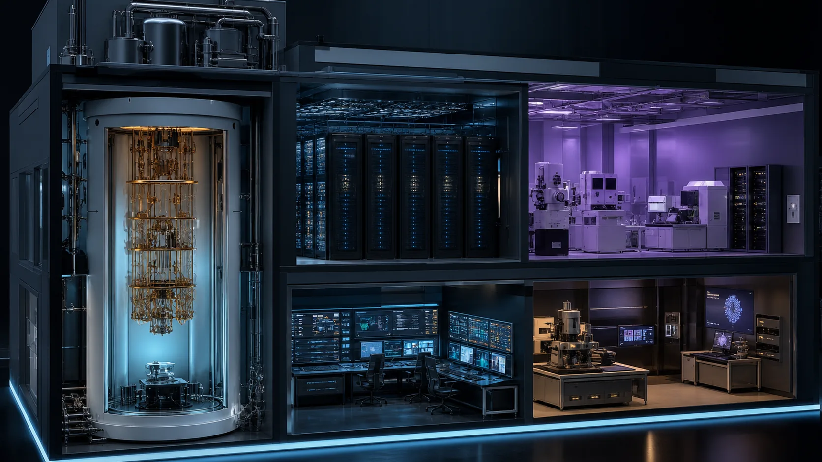
defining parameter.
as a live fallback carrying a pre-written trigger. The margin is thinner than the score suggests, because no like-for-like comparison exists.
2.5 million cryogenic wires and 3.6 W of heat at 100 mK.
requirement CRY-1, and it is the program.
maturity grounds, keeps qLDPC behind an explicit upgrade gate, and sizes magic-state production by cultivation rather than distillation.
both power and capital. Plan it first, not last.
per-channel control power (13.75x of published spread, straddling buildability), the distributed-overhead multiplier (1.41 erases the runtime margin), and the end-to-end reaction time (10 us needed, 63 us measured).
make is that its arithmetic is checkable, its assumptions are labelled, and both authors tried to break the other's half.